- 您現(xiàn)在的位置:買賣IC網(wǎng) > PDF目錄17043 > M52277EVB (Freescale Semiconductor)BOARD DEMO FOR MCF5227 PDF資料下載
參數(shù)資料
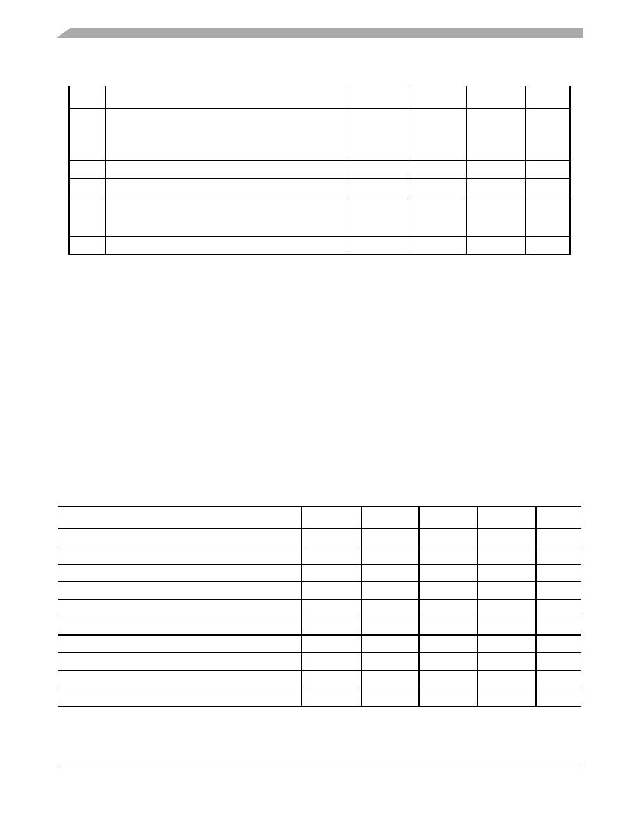
| 型號: | M52277EVB |
| 廠商: | Freescale Semiconductor |
| 文件頁數(shù): | 13/46頁 |
| 文件大小: | 0K |
| 描述: | BOARD DEMO FOR MCF5227 |
| 標準包裝: | 1 |
| 系列: | ColdFire® |
| 類型: | MCU |
| 適用于相關(guān)產(chǎn)品: | MCF52277 |
| 所含物品: | 板 |
第1頁第2頁第3頁第4頁第5頁第6頁第7頁第8頁第9頁第10頁第11頁第12頁當前第13頁第14頁第15頁第16頁第17頁第18頁第19頁第20頁第21頁第22頁第23頁第24頁第25頁第26頁第27頁第28頁第29頁第30頁第31頁第32頁第33頁第34頁第35頁第36頁第37頁第38頁第39頁第40頁第41頁第42頁第43頁第44頁第45頁第46頁
MCF5227x ColdFire Microprocessor Data Sheet, Rev. 8
Electrical Characteristics
Freescale Semiconductor
20
5.6
ASP Electrical Characteristics
Table 12 lists the electrical specifications for the ASP module.
13
Discrete load capacitance for XTAL
Discrete load capacitance for EXTAL
CL_XTAL
CL_EXTAL
—2
× (C
L –
CS_XTAL –
CS_EXTAL –
CS_PCB)
7
pF
14
Frequency un-LOCK Range
fUL
–4.0
4.0
% fsys
15
Frequency LOCK Range
fLCK
–2.0
2.0
% fsys
17
Peak-to-peak jitter (Clock edge to clock edge)
Long-term jitter
Cjitter
—
10
TBD
% fsys/2
19
VCO frequency (fvco = fref × PFDR)
fvco
350
540
MHz
1 Although these are the allowable frequency ranges, do not violate the VCO frequency range of the PLL. See the
MCF5227x Reference Manual for more details.
2 The minimum system frequency is the minimum input clock divided by the maximum low-power divider
(16 MHz
÷ 32,768). When the PLL is enabled, the minimum system frequency (f
sys) is 37.5 MHz.
3 This parameter is guaranteed by characterization before qualification rather than 100% tested. Applies to external clock
reference only.
4 Proper PC board layout procedures must be followed to achieve specifications.
5 This parameter is guaranteed by design rather than 100% tested.
6 This specification is the PLL lock time only and does not include oscillator start-up time..
7
CS_PCB is the measured PCB stray capacitance on EXTAL and XTAL.
8
Jitter is the average deviation from the programmed frequency measured over the specified interval at maximum fsys.
Measurements are made with the device powered by filtered supplies and clocked by a stable external clock signal.
Noise injected into the PLL circuitry via PLL VDD, EVDD, and VSS and variation in crystal oscillator frequency increase
the Cjitter percentage for a given interval.
Table 12. ASP Electrical Characteristics
Characteristic
Symbol
Min
Typical
Max
Unit
ASP Analog Supply Voltage
VDDA
3.0
—
3.6
V
Input Voltage Range
VADIN
0—
VDDA
V
Operating Current Consumption
IDDA_ON
—
700
—
uA
Power-down Current Consumption
IDDA_OFF
—1
—
uA
Resolution
RES
——12
bits
Sampling rate
—
125
kS/s
Integral Non-linearity
INL
—
±8
±24
lsb1
Differential Non-linearity
DNL
—
±2
±24
ADC Internal Clock Frequency
tAIC
2—
8
MHz
Conversion Range
RAD
0—
VDDA
V
Table 11. PLL Electrical Characteristics (continued)
Num
Characteristic
Symbol
Min
Max
Unit
相關(guān)PDF資料 |
PDF描述 |
|---|---|
| 0210490925 | CABLE JUMPER 1.25MM .076M 23POS |
| ECM12DSEH-S13 | CONN EDGECARD 24POS .156 EXTEND |
| VI-J1R-EY | CONVERTER MINIMOD DC/DC 7.5V 50W |
| VE-21T-EY | CONVERTER MOD DC/DC 6.5V 50W |
| 0210490924 | CABLE JUMPER 1.25MM .076M 23POS |
相關(guān)代理商/技術(shù)參數(shù) |
參數(shù)描述 |
|---|---|
| M5228FP | 制造商:Panasonic Industrial Company 功能描述:IC |
| M5228P | 制造商:Panasonic Industrial Company 功能描述:IC |
| M5229 | 制造商:Panasonic Industrial Company 功能描述:DISCD IC |
| M-522CT | 制造商:NEC 制造商全稱:NEC 功能描述:DC Line Fileters |
| M522D | 制造商:GOSSEN METRAWATT 功能描述:PSI MODULE PROFITEST PSI-BC |
發(fā)布緊急采購,3分鐘左右您將得到回復。