- 您現(xiàn)在的位置:買賣IC網(wǎng) > PDF目錄370961 > M44C090 (TEMIC SEMICONDUCTORS) Low-Current Microcontroller for Wireless Communication PDF資料下載
參數(shù)資料
| 型號: | M44C090 |
| 廠商: | TEMIC SEMICONDUCTORS |
| 元件分類: | 微控制器/微處理器 |
| 英文描述: | Low-Current Microcontroller for Wireless Communication |
| 中文描述: | 4-BIT, MROM, MICROCONTROLLER, PDSO20 |
| 封裝: | SSOP-20 |
| 文件頁數(shù): | 19/63頁 |
| 文件大小: | 503K |
| 代理商: | M44C090 |
第1頁第2頁第3頁第4頁第5頁第6頁第7頁第8頁第9頁第10頁第11頁第12頁第13頁第14頁第15頁第16頁第17頁第18頁當(dāng)前第19頁第20頁第21頁第22頁第23頁第24頁第25頁第26頁第27頁第28頁第29頁第30頁第31頁第32頁第33頁第34頁第35頁第36頁第37頁第38頁第39頁第40頁第41頁第42頁第43頁第44頁第45頁第46頁第47頁第48頁第49頁第50頁第51頁第52頁第53頁第54頁第55頁第56頁第57頁第58頁第59頁第60頁第61頁第62頁第63頁

M44C890
M44C090
Rev.A4, 14-Dec-01
19 (63)
3
3.1
Peripheral Modules
Addressing Peripherals
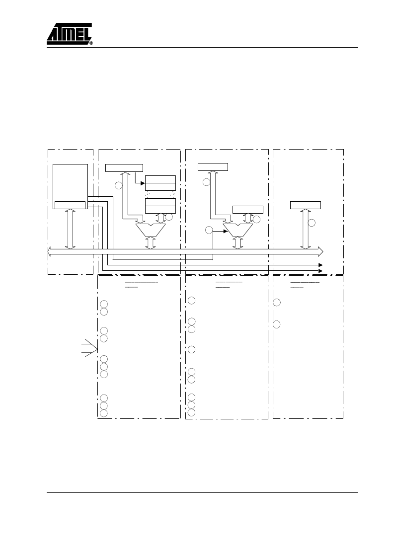
Accessing the peripheral modules takes place via the I/O
bus (see figure 21). The IN or OUT instructions allow di-
rect addressing of up to 16 I/O modules. A dual register
addressing scheme has been adopted to enable direct ad-
dressing of the
”
primary register
”
. To address the
”
auxiliary register
”
, the access must be switched with an
”
auxiliary switching module
”
. Thus a single IN (or OUT)
to the module address will read (or write) into the module
Module ASW
primary register. Accessing the auxiliary register is per-
formed with the same instruction preceded by writing the
module address into the auxiliary switching module. Byte
wide registers are accessed by multiple IN- (or OUT-)
instructions. For more complex peripheral modules, with
a larger number of registers, extended addressing is used.
In this case a bank of up to 16 subport registers are indi-
rectly addressed with the subport address. The first
OUT-instruction writes the subport address to the sub-
address register, the second IN- or OUT-instruction reads
data from or writes data to the addressed subport.
Subaddress Reg.
Subport 0
Subport 1
Subport Fh
Subport Eh
I/O bus
Aux. Reg.
Primary Reg.
Bank of
Primary Regs.
Primary Reg.
Primary Reg.
(Address Pointer)
Auxiliary Switch
Module
Indirect Subport
Access
Dual Register
Access
Single Register
Access
to other modules
Address(M2) Address(ASW) OUT
Aux._Data Address(M2) OUT
Prim._Data Address(M2) OUT
(Primary Register Write)
Prim._Data Address(M3) OUT
(Primary Register Write)
Addr.(SPort) Addr.(M1) OUT
SPort_Data Addr.(M1) OUT
1
2
(Subport Register Write)
3
4
5
1
2
3
6
6
4
5
Example of
qFORTH
Program
Code
Addr.(Mx) = Module Mx Address
Addr.(SPort) = Subport Address
Aux._Data = data to be written into Auxiliary Register
Aux._Data (lo)= data to be written into Auxiliary Register (low nibble)
Prim._Data = data to be written into Primary Register.
Addr.(SPort) Addr.(M1) OUT
1
2
(Subport Register Read)
(Subport Register Write Byte)
Addr.(M1) IN
Address(M2) Address(ASW) OUT
Address(M2) IN
(Auxiliary Register Read)
4
5
Address(M2) IN
(Primary Register Read)
3
Address(M3) IN
(Primary Register Read)
6
Addr.(ASW) = Auxiliary Switch Module Address
Addr.(SPort) Addr.(M1) OUT
SPort_Data(lo) Addr.(M1) OUT
SPort_Data(hi) Addr.(M1) OUT
1
2
2
Addr.(SPort) Addr.(M1) OUT
Addr.(M1) IN
Addr.(M1) IN
1
2
2
(Subport Register Read Byte)
SPort_Data(lo) = data to be written into SubPort (low nibble)
SPort_Data(hi) = data to be written into Subport (high nibble)
(lo) = SPort_Data (low nibble)
(hi) = SPort_Data (high nibble)
Address(M2) Address(ASW) OUT
Aux._Data(lo) Address(M2) OUT
Aux._Data(hi) Address(M2) OUT
(Auxiliary Register Write Byte)
4
5
5
Aux._Data (hi) = data to be written into Auxiliary Register(high nibble)
( Auxiliary Register Write )
13357
(hi)
(lo)
Module M1
Module M2
Module M3
Figure 21. Example of I/O addressing
相關(guān)PDF資料 |
PDF描述 |
|---|---|
| M44C090-H | Low-Current Microcontroller for Wireless Communication |
| M44C890 | Low-Current Microcontroller for Wireless Communication |
| M44C890-H | Low-Current Microcontroller for Wireless Communication |
| M4N25 | 6-Pin DIP Optoisolators Transistor Output |
| M4N26 | 6-Pin DIP Optoisolators Transistor Output |
相關(guān)代理商/技術(shù)參數(shù) |
參數(shù)描述 |
|---|---|
| M44C090-H | 制造商:ATMEL 制造商全稱:ATMEL Corporation 功能描述:Low-Current Microcontroller for Wireless Communication |
| M44C890 | 制造商:ATMEL 制造商全稱:ATMEL Corporation 功能描述:Low-Current Microcontroller for Wireless Communication |
| M44C890-H | 制造商:ATMEL 制造商全稱:ATMEL Corporation 功能描述:Low-Current Microcontroller for Wireless Communication |
| M44S05K4F1 | 功能描述:汽車連接器 MX44 Terminals RoHS:否 制造商:Amphenol SINE Systems 產(chǎn)品:Contacts 系列:ATP 位置數(shù)量: 型式:Female 安裝風(fēng)格: 端接類型: 觸點電鍍:Nickel |
| M44T332538880MHZ | 制造商:MEC 功能描述: |
發(fā)布緊急采購,3分鐘左右您將得到回復(fù)。