- 您現(xiàn)在的位置:買賣IC網(wǎng) > PDF目錄67763 > M37643F8FP 8-BIT, FLASH, 12 MHz, MICROCONTROLLER, PQFP80 PDF資料下載
參數(shù)資料
| 型號: | M37643F8FP |
| 元件分類: | 微控制器/微處理器 |
| 英文描述: | 8-BIT, FLASH, 12 MHz, MICROCONTROLLER, PQFP80 |
| 封裝: | 14 X 20 MM, 0.80 MM PITCH, PLASTIC, QFP-80 |
| 文件頁數(shù): | 108/120頁 |
| 文件大?。?/td> | 1253K |
| 代理商: | M37643F8FP |
第1頁第2頁第3頁第4頁第5頁第6頁第7頁第8頁第9頁第10頁第11頁第12頁第13頁第14頁第15頁第16頁第17頁第18頁第19頁第20頁第21頁第22頁第23頁第24頁第25頁第26頁第27頁第28頁第29頁第30頁第31頁第32頁第33頁第34頁第35頁第36頁第37頁第38頁第39頁第40頁第41頁第42頁第43頁第44頁第45頁第46頁第47頁第48頁第49頁第50頁第51頁第52頁第53頁第54頁第55頁第56頁第57頁第58頁第59頁第60頁第61頁第62頁第63頁第64頁第65頁第66頁第67頁第68頁第69頁第70頁第71頁第72頁第73頁第74頁第75頁第76頁第77頁第78頁第79頁第80頁第81頁第82頁第83頁第84頁第85頁第86頁第87頁第88頁第89頁第90頁第91頁第92頁第93頁第94頁第95頁第96頁第97頁第98頁第99頁第100頁第101頁第102頁第103頁第104頁第105頁第106頁第107頁當(dāng)前第108頁第109頁第110頁第111頁第112頁第113頁第114頁第115頁第116頁第117頁第118頁第119頁第120頁
88
7643 Group
SINGLE-CHIP 8-BIT CMOS MICROCOMPUTER
MITSUBISHI MICROCOMPUTERS
PRELIMINAR
Y
Notice:
This
is not
a final
specification.
Some
parametric
limits
are
subject
to
change.
Outline Performance (CPU Rewrite Mode)
CPU rewrite mode is usable in the single-chip, memory expansion
or Boot mode. The only User ROM area can be rewritten in CPU
rewrite mode.
In CPU rewrite mode, the CPU erases, programs and reads the in-
ternal flash memory by executing software commands. This
rewrite control program must be transferred to a memory such as
the internal RAM before it can be executed.
The MCU enters CPU rewrite mode by applying 4.50 V to 5.25 V
to the CNVSS pin and setting “1” to the CPU Rewrite Mode Select
Bit (bit 1 of address 006A16). Software commands are accepted
once the mode is entered.
Use software commands to control program and erase operations.
Whether a program or erase operation has terminated normally or
in error can be verified by reading the status register.
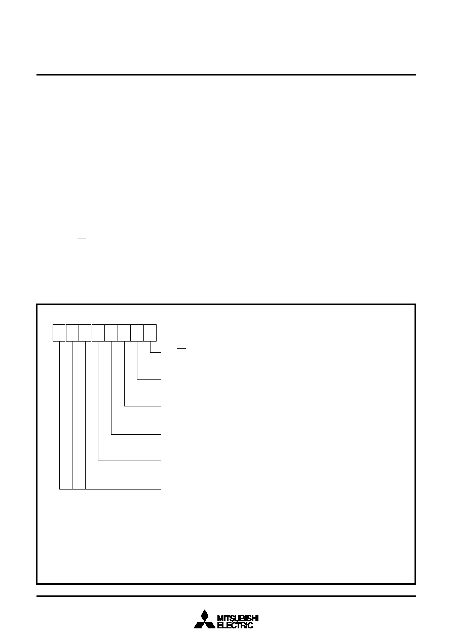
Figure 79 shows the flash memory control register.
Bit 0 is the RY/BY status flag used exclusively to read the operat-
ing status of the flash memory. During programming and erase
operations, it is “0” (busy). Otherwise, it is “1” (ready).
Bit 1 is the CPU Rewrite Mode Select Bit. When this bit is set to
“1”, the MCU enters CPU rewrite mode. Software commands are
accepted once the mode is entered. In CPU rewrite mode, the
Flash memory control register (address 006A16)
FMCR
RY/BY status flag
0: Busy (being programmed or erased)
1: Ready
CPU rewrite mode select bit (Note 2)
0: Normal mode (Software commands invalid)
1: CPU rewrite mode (Software commands acceptable)
CPU rewrite mode entry flag
0: Normal mode
1: CPU rewrite mode
Flash memory reset bit (Note 3)
0: Normal operation
1: Reset
User ROM area / Boot ROM area select bit (Note 4)
0: User ROM area accessed
1: Boot ROM area accessed
Reserved bits (Indefinite at read/ “0” at write)
b0
b7
Notes 1: The contents of flash memory control register are “XXX00001” just after reset release.
2: For this bit to be set to “1”, the user needs to write “0” and then “1” to it in succession. If it is not
this procedure, this bit will not be set to ”1”. Additionally, it is required to ensure that no interrupt
will be generated during that interval.
Use the control program in the area except the built-in flash memory for write to this bit.
3: This bit is valid when the CPU rewrite mode select bit is “1”. Set this bit 3 to “0” subsequently after
setting bit 3 to “1”.
4: Use the control program in the area except the built-in flash memory for write to this bit.
CPU becomes unable to access the internal flash memory directly.
Therefore, use the control program in a memory other than inter-
nal flash memory for write to bit 1. To set this bit to “1”, it is
necessary to write “0” and then write “1” in succession. The bit can
be set to “0” by only writing “0”.
Bit 2 is the CPU Rewrite Mode Entry Flag. This flag indicates “1” in
CPU rewrite mode, so that reading this flag can check whether
CPU rewrite mode has been entered or not.
Bit 3 is the flash memory reset bit used to reset the control circuit
of internal flash memory. This bit is used when exiting CPU rewrite
mode and when flash memory access has failed. When the CPU
Rewrite Mode Select Bit is “1”, setting “1” for this bit resets the
control circuit. To set this bit to “1”, it is necessary to write “0” and
then write “1” in succession. To release the reset, it is necessary
to set this bit to “0”.
Bit 4 is the User Area/Boot Area Select Bit. When this bit is set to
“1”, Boot ROM area is accessed, and CPU rewrite mode in Boot
ROM area is available. In Boot mode, this bit is set to “1” auto-
matically. Reprogramming of this bit must be in a memory other
than internal flash memory.
Figure 80 shows a flowchart for setting/releasing CPU rewrite
mode.
Fig. 79 Structure of flash memory control register
相關(guān)PDF資料 |
PDF描述 |
|---|---|
| M37643F8HP | 8-BIT, FLASH, 12 MHz, MICROCONTROLLER, PQFP80 |
| M37643M8-XXXHP | 8-BIT, MROM, 12 MHz, MICROCONTROLLER, PQFP80 |
| M37702S1LGP | 16-BIT, 8 MHz, MICROCONTROLLER, PQFP80 |
| M37702M2LXXXGP | 16-BIT, MROM, 8 MHz, MICROCONTROLLER, PQFP80 |
| M37702M2LXXXHP | 16-BIT, MROM, 8 MHz, MICROCONTROLLER, PQFP80 |
相關(guān)代理商/技術(shù)參數(shù) |
參數(shù)描述 |
|---|---|
| M37643F8M8-XXXFP | 制造商:RENESAS 制造商全稱:Renesas Technology Corp 功能描述:SINGLE-CHIP 8-BIT CMOS MICROCOMPUTER |
| M37643M8E8-XXXFP | 制造商:RENESAS 制造商全稱:Renesas Technology Corp 功能描述:SINGLE-CHIP 8-BIT CMOS MICROCOMPUTER |
| M37643M8M8-XXXFP | 制造商:RENESAS 制造商全稱:Renesas Technology Corp 功能描述:SINGLE-CHIP 8-BIT CMOS MICROCOMPUTER |
| M3764A-12 | 制造商:OK International 功能描述: |
| M3765 | 制造商:未知廠家 制造商全稱:未知廠家 功能描述:HORN/SIREN WITH SOFT CHIRP 6 ALARM SOUNDS |
發(fā)布緊急采購,3分鐘左右您將得到回復(fù)。