- 您現(xiàn)在的位置:買賣IC網(wǎng) > PDF目錄377801 > M13S256328A (Elite Semiconductor Memory Technology Inc.) 2M x 32 Bit x 4 Banks Double Data Rate SDRAM PDF資料下載
參數(shù)資料
| 型號(hào): | M13S256328A |
| 廠商: | Elite Semiconductor Memory Technology Inc. |
| 英文描述: | 2M x 32 Bit x 4 Banks Double Data Rate SDRAM |
| 中文描述: | 200萬× 32位× 4個(gè)銀行雙倍數(shù)據(jù)速率SDRAM |
| 文件頁數(shù): | 22/47頁 |
| 文件大小: | 807K |
| 代理商: | M13S256328A |
第1頁第2頁第3頁第4頁第5頁第6頁第7頁第8頁第9頁第10頁第11頁第12頁第13頁第14頁第15頁第16頁第17頁第18頁第19頁第20頁第21頁當(dāng)前第22頁第23頁第24頁第25頁第26頁第27頁第28頁第29頁第30頁第31頁第32頁第33頁第34頁第35頁第36頁第37頁第38頁第39頁第40頁第41頁第42頁第43頁第44頁第45頁第46頁第47頁
ES MT
M13S256328A
Elite Semiconductor Memory Technology Inc.
Publication Date : May. 2007
Revision : 1.2 22/47
1. For the earliest possible Precharge command following a Write burst without interrupting the burst, the minimum time for
write recovery is defined by t
WR
.
2. When a precharge command interrupts a Write burst operation, the data mask pin, DQ, is used to mask input data during
the time between the last valid write data and the rising clock edge in which the Precharge command is given. During this
time, the DQS input is still required to strobe in the state of DM.
The minimum time for write recovery is defined by t
WR
.
3. For a Write with autoprecharge command, a new Bank Activate command may be issued to the same bank after t
WR
+ t
RP
where t
WR
+ t
RP
starts on the falling DQS edge that strobed in the last valid data and ends on the rising clock edge that
strobes in the Bank Activate commands. During write with autoprecharge, the initiation of the internal precharge occurs at
the same time as the earliest possible external Precharge command without interrupting the Write burst as described in 1
above.
4. In all cases, a Precharge operation cannot be initiated unless t
RAS
(min) [minimum Bank Activate to Precharge time] has
been satisfied. This includes Write with autoprecharge commands where t
RAS
(min) must still be satisfied such that a Write
with autoprecharge command has the same timing as a Write command followed by the earliest possible Precharge
command which does not interrupt the burst.
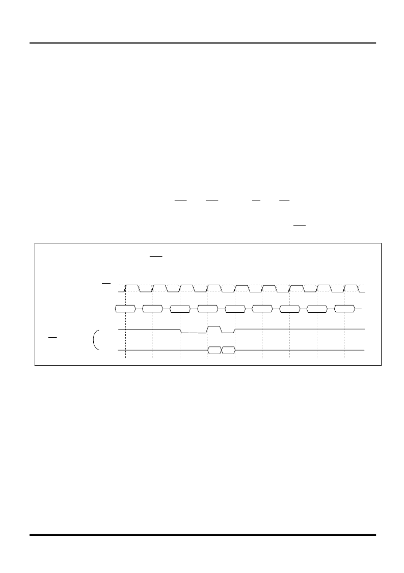
Burst Stop
The burst stop command is initiated by having RAS and CAS high with CS and
WE
low at the rising edge of the
clock (CLK). The burst stop command has the fewest restriction making it the easiest method to use when terminating a burst
read operation before it has been completed. When the burst stop command is issued during a burst read cycle, the pair of
data and DQS (Data Strobe) go to a high impedance state after a delay which is equal to the CAS latency set in the mode
register. The burst stop command, however, is not supported during a write burst operation.
<Burst Length = 4, CAS Latency = 3 >
0
1
2
CL K
CL K
3
4
5
6
7
8
COMMAND
READ A
NOP
NOP
NOP
NOP
NOP
NOP
NOP
Burst Stop
CA S Lat en cy = 3
DQS
DQ's
Dout 0 Dout 1
相關(guān)PDF資料 |
PDF描述 |
|---|---|
| M13S32321A | 256K x 32 Bit x 4 Banks Double Data Rate SDRAM |
| M13S64164A-6BG | 1M x 16 Bit x 4 Banks Double Data Rate SDRAM |
| M13S64164A | 1M x 16 Bit x 4 Banks Double Data Rate SDRAM |
| M13S64164A-5BG | 1M x 16 Bit x 4 Banks Double Data Rate SDRAM |
| M13S64164A-5TG | 1M x 16 Bit x 4 Banks Double Data Rate SDRAM |
相關(guān)代理商/技術(shù)參數(shù) |
參數(shù)描述 |
|---|---|
| M13S256328A-5BG | 制造商:ESMT 制造商全稱:Elite Semiconductor Memory Technology Inc. 功能描述:2M x 32 Bit x 4 Banks Double Data Rate SDRAM |
| M13S32321A | 制造商:ESMT 制造商全稱:Elite Semiconductor Memory Technology Inc. 功能描述:256K x 32 Bit x 4 Banks Double Data Rate SDRAM |
| M13S32321A_08 | 制造商:ESMT 制造商全稱:Elite Semiconductor Memory Technology Inc. 功能描述:256K x 32 Bit x 4 Banks Double Data Rate SDRAM |
| M13S32321A-5L | 制造商:ESMT 制造商全稱:Elite Semiconductor Memory Technology Inc. 功能描述:256K x 32 Bit x 4 Banks Double Data Rate SDRAM |
| M13S32321A-6L | 制造商:ESMT 制造商全稱:Elite Semiconductor Memory Technology Inc. 功能描述:256K x 32 Bit x 4 Banks Double Data Rate SDRAM |
發(fā)布緊急采購,3分鐘左右您將得到回復(fù)。