- 您現(xiàn)在的位置:買賣IC網(wǎng) > PDF目錄180051 > M-ORSO82G52BM680-DB (LATTICE SEMICONDUCTOR CORP) FPGA, 1296 CLBS, 333000 GATES, PBGA680 PDF資料下載
參數(shù)資料
| 型號: | M-ORSO82G52BM680-DB |
| 廠商: | LATTICE SEMICONDUCTOR CORP |
| 元件分類: | FPGA |
| 英文描述: | FPGA, 1296 CLBS, 333000 GATES, PBGA680 |
| 封裝: | PLASTIC, FBGA-680 |
| 文件頁數(shù): | 76/123頁 |
| 文件大小: | 2207K |
| 代理商: | M-ORSO82G52BM680-DB |
第1頁第2頁第3頁第4頁第5頁第6頁第7頁第8頁第9頁第10頁第11頁第12頁第13頁第14頁第15頁第16頁第17頁第18頁第19頁第20頁第21頁第22頁第23頁第24頁第25頁第26頁第27頁第28頁第29頁第30頁第31頁第32頁第33頁第34頁第35頁第36頁第37頁第38頁第39頁第40頁第41頁第42頁第43頁第44頁第45頁第46頁第47頁第48頁第49頁第50頁第51頁第52頁第53頁第54頁第55頁第56頁第57頁第58頁第59頁第60頁第61頁第62頁第63頁第64頁第65頁第66頁第67頁第68頁第69頁第70頁第71頁第72頁第73頁第74頁第75頁當(dāng)前第76頁第77頁第78頁第79頁第80頁第81頁第82頁第83頁第84頁第85頁第86頁第87頁第88頁第89頁第90頁第91頁第92頁第93頁第94頁第95頁第96頁第97頁第98頁第99頁第100頁第101頁第102頁第103頁第104頁第105頁第106頁第107頁第108頁第109頁第110頁第111頁第112頁第113頁第114頁第115頁第116頁第117頁第118頁第119頁第120頁第121頁第122頁第123頁

Lattice Semiconductor
ORCA ORSO82G5 Data Sheet
56
IPC2_B1 combines links from channels BA,BB
IPC2_B2 combines links from channels BC,BD
The IPC8 block combines cells from all 8 aligned links and transmits them to the FPGA logic.
Before an IPC can begin reading data from the RXFIFOs and assembling cells, it must rst align all FIFOs in a port
bundle. This is accomplished by handshaking signals between the framer and IPC. The framer indicates to the IPC
that framing has been acquired.The behavior of the IPC is dependent on the AUTO_BUNDLE register bit. If
AUTO_BUNDLE is set for all links in a bundle, the link is brought up when the link is considered good by the fram-
ers. If AUTO_BUNDLE is not set, all links in the bundle must be valid before the link is brought up. The framer does
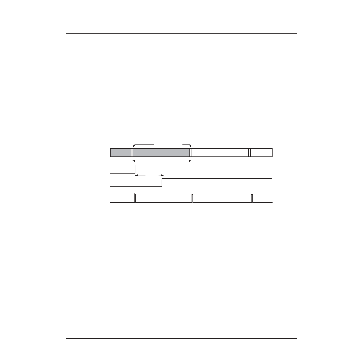
not start lling the FIFOs, however, until the next A1/A2 SONET signal.
As shown in Figure 41, the FIFOs are not ready to be read by the IPC until 60 s after all links in a code group is
up. This ensures that all cells are aligned coming out of the FIFOs for the code group.
Figure 41. Frame Start-up Timing
The next thing the IPC must do is determine when the reads may begin. Before reading any data from a FIFO, the
FIFO must have a full cell available to be read. This is indicated by each FIFO and is registered by the IPC. The IPC
then makes sure that the cells in a given port are received in the order that they are transmitted
The twin-link IPC2 blocks can be run at 1/4 the of 156 MHz rate (39 MHz) since each block parses cells from only
two-links. A 4:1 MUX is used for each IPC2 block to provide a 40-bit bus at 156 MHz across the boundary.
IPC Receive Cell Mode Timing Core/FPGA
This section contains timing diagrams for major interfaces of this block to the FPGA logic when cells are to be
transferred. Figure 42 shows the cell twin-link mode timing. The number of clock cycles to transfer the cell data
depends on the payload size enabled. Error indications for CELL BIP errors and CELL DROP are also shown.
~60
S
HEAD_OF_FRAME
Data
RX_LINK_GOOD
Receive Frame
A1/A2 Framing Byte
RX_FIFO_EN
Frame = 125
S
Data
Cell Data is Ignored, and FIFOs are Empty Until
First Cell in Frame after RX_FIFO_EN goes High
相關(guān)PDF資料 |
PDF描述 |
|---|---|
| M-ORT82G51BM680-DB | FPGA, 1296 CLBS, 333000 GATES, PBGA680 |
| M-ORT82G52BM680-DB | FPGA, 1296 CLBS, 333000 GATES, PBGA680 |
| M.PI-1R1D12 | 1 ELEMENT, 1.1 uH, GENERAL PURPOSE INDUCTOR, SMD |
| M01-014-1452PA | 14 CONTACT(S), MALE, RIGHT ANGLE TELECOM AND DATACOM CONNECTOR, SOLDER |
| M01-016-1443PA | 16 CONTACT(S), MALE, RIGHT ANGLE TELECOM AND DATACOM CONNECTOR, SOLDER |
相關(guān)代理商/技術(shù)參數(shù) |
參數(shù)描述 |
|---|---|
| MORTAR-44LB | 制造商:3M Electronic Products Division 功能描述:3M(TM) FIRE BARRIER MORTAR, 44 98040056073 制造商:3M Electronic Products Division 功能描述:Fire Barrier 44 lb Bag |
| MO-RX3930 | 制造商:未知廠家 制造商全稱:未知廠家 功能描述:FSK RECEIVER MODULE |
| MO-RX3930-FS | 制造商:未知廠家 制造商全稱:未知廠家 功能描述:FSK RECEIVER MODULE |
| MO-RX3930-FS315M | 制造商:未知廠家 制造商全稱:未知廠家 功能描述:FSK RECEIVER MODULE |
| MO-RX3930-FS434M | 制造商:未知廠家 制造商全稱:未知廠家 功能描述:FSK RECEIVER MODULE |
發(fā)布緊急采購,3分鐘左右您將得到回復(fù)。