- 您現(xiàn)在的位置:買賣IC網(wǎng) > PDF目錄377727 > LTAEY (Linear Integrated Systems) Differential Input 16-Bit No Latency DS ADC PDF資料下載
參數(shù)資料
| 型號: | LTAEY |
| 廠商: | Linear Integrated Systems |
| 英文描述: | Differential Input 16-Bit No Latency DS ADC |
| 中文描述: | 差分輸入16位ADC的無延遲局副局長 |
| 文件頁數(shù): | 5/28頁 |
| 文件大小: | 298K |
| 代理商: | LTAEY |
第1頁第2頁第3頁第4頁當(dāng)前第5頁第6頁第7頁第8頁第9頁第10頁第11頁第12頁第13頁第14頁第15頁第16頁第17頁第18頁第19頁第20頁第21頁第22頁第23頁第24頁第25頁第26頁第27頁第28頁
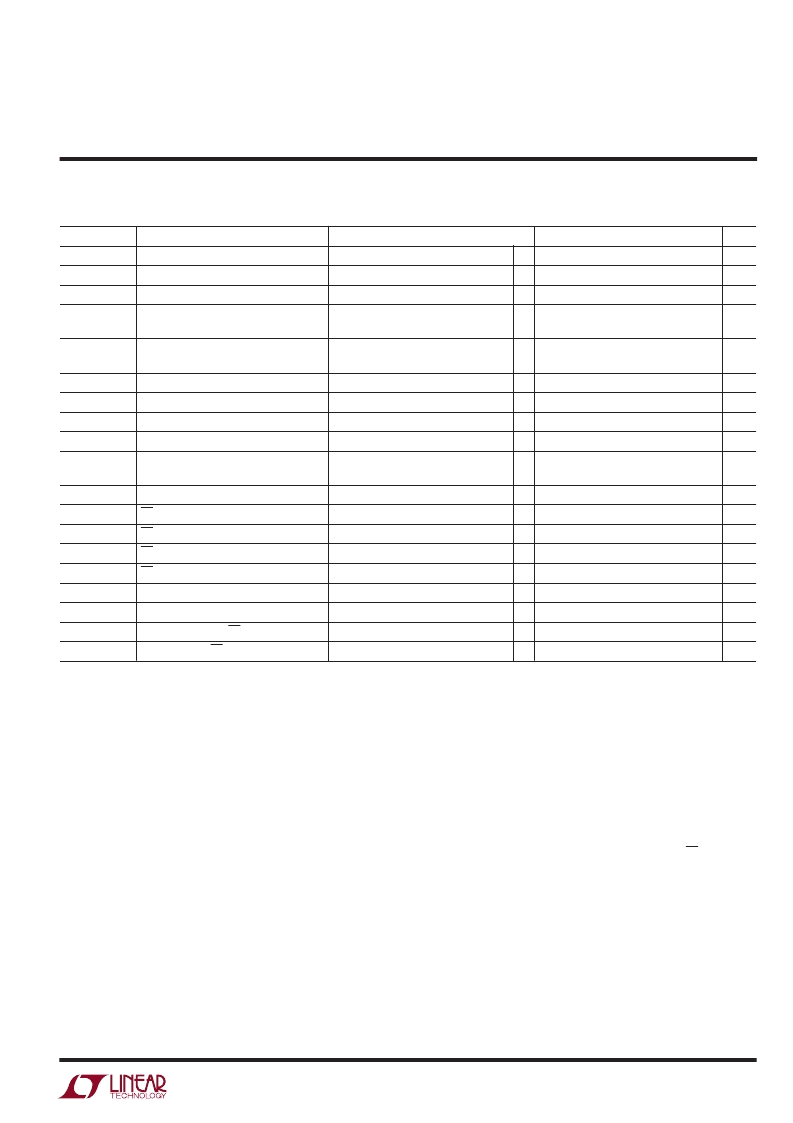
LTC2433-1
5
24331fa
Note 9:
The converter is in internal SCK mode of operation such that
the SCK pin is used as digital output. In this mode of operation the
SCK pin has a total equivalent load capacitance C
LOAD
= 20pF.
Note 10:
The external oscillator is connected to the F
O
pin. The external
oscillator frequency, f
EOSC
, is expressed in kHz.
Note 11:
The converter uses the internal oscillator.
F
O
= 0V.
Note 12:
1.45
μ
V RMS noise is independent of V
REF
. Since the noise
performance is limited by the quantization, lowering V
REF
improves the
effective resolution.
Note 13:
Guaranteed by design and test correlation.
Note 14:
The low sleep mode current is valid only when CS is high.
Note 15:
These parameters are guaranteed by design over the full
supply and temperature range. Automated testing procedures are
limited by the LSB step size (V
REF
/65,536).
Note 1:
Absolute Maximum Ratings are those values beyond which the
life of the device may be impaired.
Note 2:
All voltage values are with respect to GND.
Note 3:
V
CC
= 2.7V to 5.5V unless otherwise specified.
V
REF
= REF
+
– REF
–
, V
REFCM
= (REF
+
+ REF
–
)/2; V
IN
= IN
+
– IN
–
,
V
INCM
= (IN
+
+ IN
–
)/2.
Note 4:
F
O
pin tied to GND or to an external conversion clock source
with f
EOSC
= 139,800Hz unless otherwise specified.
Note 5:
Guaranteed by design, not subject to test.
Note 6:
Integral nonlinearity is defined as the deviation of a code from
a precise analog input voltage. Maximum specifications are limited by
the LSB step size (V
REF
/2
16
) and the single shot measurement. Typical
specifications are measured from the center of the quantization band.
Note 7:
F
O
= GND (internal oscillator) or f
EOSC
= 139,800Hz
±
2%
(external oscillator).
Note 8:
The converter is in external SCK mode of operation such that
the SCK pin is used as digital input. The frequency of the clock signal
driving SCK during the data output is f
ESCK
and is expressed in kHz.
SYMBOL
f
EOSC
t
HEO
t
LEO
t
CONV
PARAMETER
External Oscillator Frequency Range
External Oscillator High Period
External Oscillator Low Period
Conversion Time
CONDITIONS
MIN
2.56
0.25
0.25
143.8
TYP
MAX
2000
390
390
149.6
UNITS
kHz
G
G
μ
s
μ
s
ms
ms
kHz
kHz
%
kHz
ns
ns
ms
ms
ms
ns
ns
ns
ns
ns
ns
ns
ns
G
F
O
= 0V
External Oscillator (Note 10)
Internal Oscillator (Note 9)
External Oscillator (Notes 9, 10)
(Note 9)
(Note 8)
(Note 8)
(Note 8)
Internal Oscillator (Notes 9, 11)
External Oscillator (Notes 9, 10)
(Note 8)
G
G
146.7
20510/f
EOSC
(in kHz)
17.5
f
EOSC
/8
f
ISCK
Internal SCK Frequency
D
ISCK
f
ESCK
t
LESCK
t
HESCK
t
DOUT_ISCK
Internal SCK Duty Cycle
External SCK Frequency Range
External SCK Low Period
External SCK High Period
Internal SCK 19-Bit Data Output Time
G
45
55
2000
G
G
250
250
1.06
G
G
G
1.09
1.11
152/f
EOSC
(in kHz)
19/f
ESCK
(in kHz)
t
DOUT_ESCK
t
1
t2
t3
t4
t
KQMAX
t
KQMIN
t
5
t
6
External SCK 19-Bit Data Output Time
CS
↓
to SDO Low Z
CS
↑
to SDO High Z
CS
↓
to SCK
↓
CS
↓
to SCK
↑
SCK
↓
to SDO Valid
SDO Hold After SCK
↓
SCK Set-Up Before CS
↓
SCK Hold After CS
↓
G
G
0
0
0
200
200
200
G
(Note 9)
(Note 8)
G
G
50
G
220
(Note 5)
G
15
50
G
G
50
The
G
denotes specifications which apply over the full operating temperature
range, otherwise specifications are at T
A
= 25
°
C. (Note 3)
TI I G CHARACTERISTICS
U
W
相關(guān)PDF資料 |
PDF描述 |
|---|---|
| LTAEZ | Differential Input 16-Bit No Latency DS ADC |
| LTC2433-1 | Differential Input 16-Bit No Latency DS ADC |
| LTC2433-1CMS | Differential Input 16-Bit No Latency DS ADC |
| LTC2433-1IMS | Differential Input 16-Bit No Latency DS ADC |
| LTC1043CS | Dual Precision Intrumentation Switched-Capacitor Building Block |
相關(guān)代理商/技術(shù)參數(shù) |
參數(shù)描述 |
|---|---|
| LTAEZ | 制造商:LINEAR 制造商全稱:LINEAR 功能描述:Differential Input 16-Bit No Latency DS ADC |
| LTAGL | 制造商:LINER 制造商全稱:Linear Technology 功能描述:100mA, Low Voltage, Very Low Dropout Linear Regulator |
| LT-ALTO350-C | 制造商:LED TEAM 功能描述:DRIVER 3CH DMX FOR RGB LED 350MA |
| LT-ALTO700-C | 制造商:LED TEAM 功能描述:LED DRIVER DC-DC CC 0.7A 制造商:LED TEAM 功能描述:LED DRIVER, DC-DC, CC, 0.7A 制造商:LED TEAM 功能描述:LED DRIVER, DC-DC, CC, 0.7A, Product Range:LED TEAM - ALTO700 Series, Input Volt 制造商:LED TEAM 功能描述:LED DRIVER, DC-DC, CC, 0.7A, Product Range:LED TEAM - ALTO700 Series, Input Voltage Min:24V, Input Voltage Max:32V, Output Current:700mA, Output Power Max:45W, DC / DC Converter Mounting:Panel, Dimming Control Type:PWM, Depth:22mm, , RoHS Compliant: Yes |
| LTALX | 制造商:Apex Tool Group 功能描述:TIP,BENT CHISEL,30 DEG,1.6MM,WP80 |
發(fā)布緊急采購,3分鐘左右您將得到回復(fù)。