- 您現(xiàn)在的位置:買賣IC網(wǎng) > PDF目錄361035 > LM9832CCVJD (NATIONAL SEMICONDUCTOR CORP) LM9832 42-Bit Color, 1200dpi USB Image Scanner PDF資料下載
參數(shù)資料
| 型號(hào): | LM9832CCVJD |
| 廠商: | NATIONAL SEMICONDUCTOR CORP |
| 元件分類: | 消費(fèi)家電 |
| 英文描述: | LM9832 42-Bit Color, 1200dpi USB Image Scanner |
| 中文描述: | SPECIALTY CONSUMER CIRCUIT, PQFP100 |
| 封裝: | PLASTIC, TQFP-100 |
| 文件頁數(shù): | 33/42頁 |
| 文件大小: | 337K |
| 代理商: | LM9832CCVJD |
第1頁第2頁第3頁第4頁第5頁第6頁第7頁第8頁第9頁第10頁第11頁第12頁第13頁第14頁第15頁第16頁第17頁第18頁第19頁第20頁第21頁第22頁第23頁第24頁第25頁第26頁第27頁第28頁第29頁第30頁第31頁第32頁當(dāng)前第33頁第34頁第35頁第36頁第37頁第38頁第39頁第40頁第41頁第42頁
33
www.national.com
8.4 High Speed Reverse
When register 07 is set to a 2, the LM9832 moves the motor
backwards at maximum speed (determined by the fast feed step-
size, registers 48 and 49) until a 0 is written to register 07 or
either one of the PAPER SENSE inputs becomes True (if that
sensor has been properly programmed to interrupt scanner
movement). The
FullSteps to Scan after PAPER SENSE 2 trips
register is not used in the High Speed Reverse mode. This func-
tion is generally used to home the sensor in flatbed scanning
applications.
The LM9832 also features a Programmed High Speed Reverse
command. This is identical to the High Speed Reverse function,
except that it will automatically stop moving once the motor has
moved the number of lines specified in registers 4A and 4B.
8.5 Short Example of a Scan
PC configures the LM9832 by writing to the configuration regis-
ters.
PC has the LM9832 scan a calibration image, then calculates
the calibration coefficients for the scanner.
PC transmits the calibration information to the LM9832.
If a sheetfed, the PC now polls the LM9832 status registers to
see if there is any paper inserted. If a flatbed, it moves the scan
head to the home position.
PC sets the Scanning bit in the Configuration Register.
PC calculates the size of the image to be scanned in bytes,
then reads bulk data from register 00 of the LM9832 until it has
read the entire image. If for some reason the scan needs to be
aborted, the PC writes a 0 to register 07.
After all image data is read, PC writes a 0 to register 07 to stop
scan.
If this is a flatbed scanner, the PC should now send a High
Speed Reverse command to send the sensor back to the home
position. For a sheetfeeder, it can send a High Speed Forward
command to eject the remainder of the image.
The scanner is now in the idle state.
9.0 Master Clock Source
The timing for the entire chip comes from the CRYSTAL OUT pin.
Typically this pin is used (with the CRYSTAL IN pin) as a crystal
oscillator. The clock frequency should be 48MHz. This 48MHz
clock is divided by the MCLK divider (register 08), and the divided
output is MCLK (Master CLocK). The MCLK divider range is from
1.0 to 32.5 in steps of 0.5. A configuration register code of 0
divides the clock by 1.0, while a code of 63 divides the clock by
32.5. AT 48MHz, this provides an MCLK range of 1.48MHz to
48MHz and a corresponding ADC conversion rate of 184kHz to
6.00MHz. This divider can be used to closely match the output
data rate to the PC’s input data rate, minimizing scan time.
MCLK is used to clock the vast majority of the LM9832’s circuits.
CRYSTAL OUT is directly used in the USB I/O section, DRAM
timing, and a few subsections where the highest possible clock
speed is required (such as the PWM pulse generator for the light
source and the stepper motors).
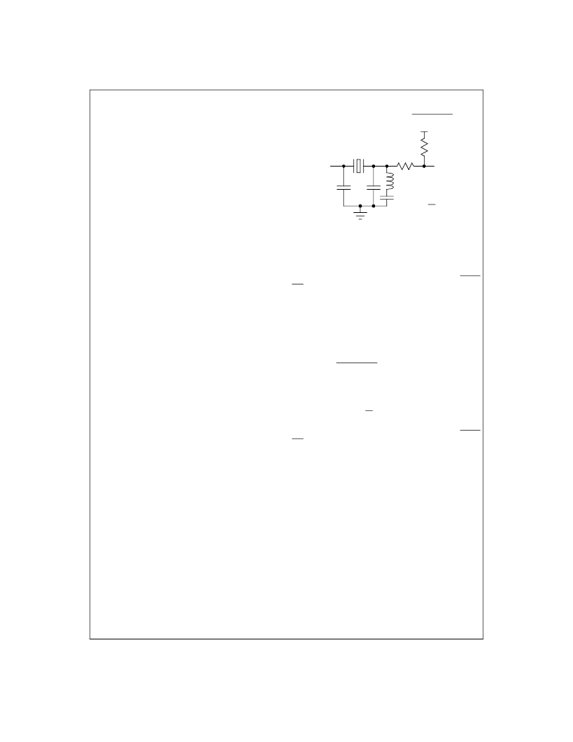
To use the LM9832’s crystal oscillator feature, tie the CRYS-
TAL/EXT CLK pin to DGND. Figure 46 shows the recommended
loading circuit and values for a 48MHz oscillator. These compo-
nent values assume 10pF of stray capacitance between CRYS-
TAL IN and ground, and 10pF between CRYSTAL OUT and
ground, for a total CRYSTAL IN and CRYSTAL OUT loading of
15pF and 25pF.
A 2.7k pullup to a 5V source is necessary to ensure oscillator
start-up. For self-powered systems, any clean source of +5V can
be used. For bus-powered systems, this pin must be connected
to the ACTIVE/SUSPENDED pin in order to meet USB suspend
power consumption requirements.
When laying out the crystal oscillator components, always keep
the traces as short as possible, to minimize stray capacitance
and inductive noise coupling, particularly on the CRYSTAL IN pin.
Operation at 24MHz (24/48 = V
D
) is not reliable and should not
be used.
To drive the LM9832 with an external 48MHz clock, tie CRYS-
TAL/EXT CLK (pin 54) to V
D
, tie CRYSTAL_IN to DGND, and
drive the TTL or CMOS-level clock signal into CRYSTAL_OUT
(pin 52).
10.0 INITIALIZATION
10.1 Power On Reset (POR)
POR is generated by the ramp of the V
A
supply pins from 0V to
+5V. A low to high to low signal on the external RESET pin will
also generate a POR. A POR event:
Resets the USB transceiver. All enumeration and configuration
data will be reset to its default setting.
The oscillator will start (or continue) oscillating.
Forces all configuration registers that have defaults (shown as
black boxes in the configuration register tables) to their default
settings (including the Reset and Standby bits). See the Reset
and Standby mode descriptions for more information.
MISC I/O 1-3 will be configured as inputs and could generate
remote wakeup signals (after the device is initialized).
MISC I/O 4-6 are configured as outputs.
Figure 46: 48 MHz Crystal Oscillator Circuit
5pF
15pF
300pF
1.2μH
CRYSTAL
IN
48MHz Third
Overtone Crystal
Ecliptek
EC-T-48.000M
C1
C2
24/48 = DGND
CRYSTAL
OUT
2.7k
ACTIVE/SUSPENDED pin
or +5V (see text)
10
22
Applications Information
(Continued)
L
相關(guān)PDF資料 |
PDF描述 |
|---|---|
| LM9832 | LM9832 42-Bit Color, 1200dpi USB Image Scanner |
| LM9833CCVJD | LM9833 48-Bit Color, 1200dpi USB Image Scanner |
| LM9833 | LM9833 48-Bit Color, 1200dpi USB Image Scanner |
| LM98501CCVBH | 10-Bit, 27 MSPS Camera Signal Processor |
| LM98501 | 10-Bit, 27 MSPS Camera Signal Processor |
相關(guān)代理商/技術(shù)參數(shù) |
參數(shù)描述 |
|---|---|
| LM9832CCVS-B | 制造商:Texas Instruments 功能描述: |
| LM9833 | 制造商:NSC 制造商全稱:National Semiconductor 功能描述:LM9833 48-Bit Color, 1200dpi USB Image Scanner |
| LM9833B-F WAF | 制造商:Texas Instruments 功能描述: |
| LM9833CCVJD | 制造商:Texas Instruments 功能描述:USB Image Scanner 100-Pin TQFP |
| LM9833CCVJD NOPB | 制造商:Texas Instruments 功能描述:Bulk |
發(fā)布緊急采購,3分鐘左右您將得到回復(fù)。