- 您現(xiàn)在的位置:買賣IC網(wǎng) > PDF目錄361035 > LM9832CCVJD (NATIONAL SEMICONDUCTOR CORP) LM9832 42-Bit Color, 1200dpi USB Image Scanner PDF資料下載
參數(shù)資料
| 型號: | LM9832CCVJD |
| 廠商: | NATIONAL SEMICONDUCTOR CORP |
| 元件分類: | 消費家電 |
| 英文描述: | LM9832 42-Bit Color, 1200dpi USB Image Scanner |
| 中文描述: | SPECIALTY CONSUMER CIRCUIT, PQFP100 |
| 封裝: | PLASTIC, TQFP-100 |
| 文件頁數(shù): | 10/42頁 |
| 文件大?。?/td> | 337K |
| 代理商: | LM9832CCVJD |
第1頁第2頁第3頁第4頁第5頁第6頁第7頁第8頁第9頁當(dāng)前第10頁第11頁第12頁第13頁第14頁第15頁第16頁第17頁第18頁第19頁第20頁第21頁第22頁第23頁第24頁第25頁第26頁第27頁第28頁第29頁第30頁第31頁第32頁第33頁第34頁第35頁第36頁第37頁第38頁第39頁第40頁第41頁第42頁
10
www.national.com
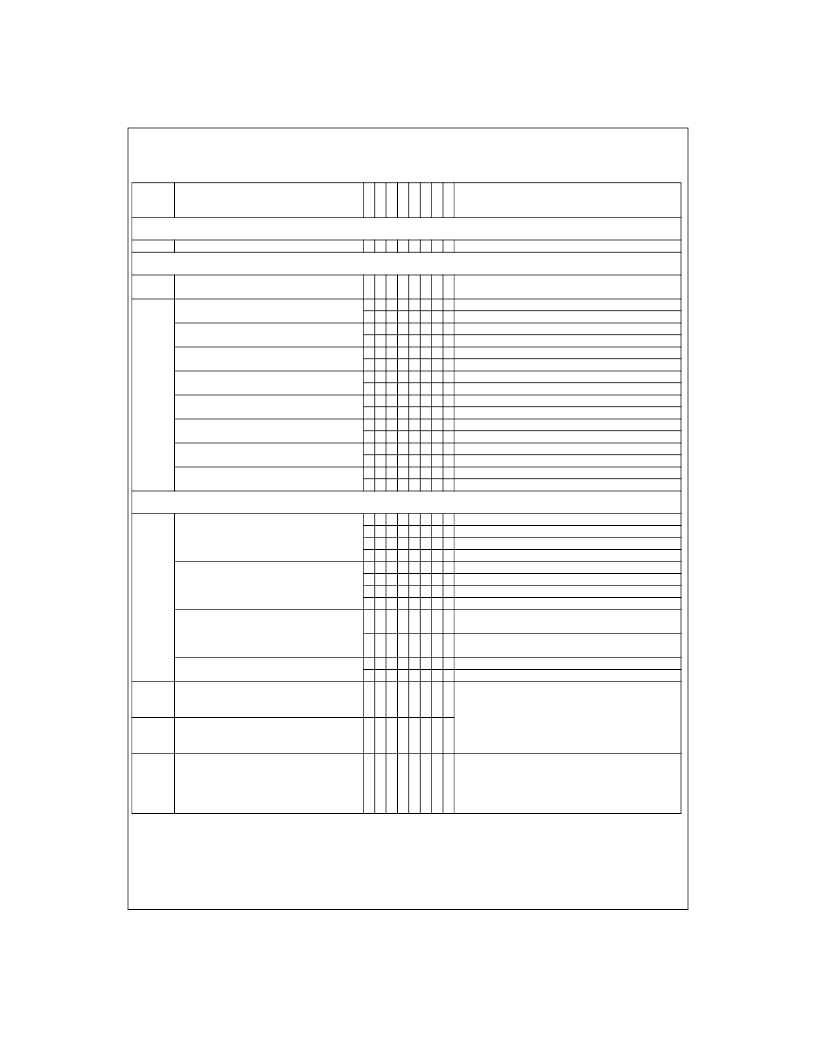
LM9832 Register Listing
Registers in bold boxes are reset to that value on power-up. All register addresses are in hexadecimal. All other numbers are
decimal unless otherwise noted.
Address
Function
D
7
D
6
D
5
D
4
D
3
D
2
D
1
D
0
Value
IMAGE BUFFER (READ ONLY)
00
Pixel (Image) Data
n n n n n n n n One byte of image data.
STATUS REGISTERS (READ ONLY)
01
Image Data Available In Buffer
n n n n n n n nkilobytes of image data is available
0 False
1 True
0
False
1
True
0
False
1
True
0
False
1
True
0
False
1
True
0
False
1
True
0
False
1
True
0
False
1
True
02
PAPER SENSE 1 State
read clears bit if edge sensitive input.
PAPER SENSE 2 State
read clears bit if edge sensitive input.
MISC I/O 1 State
read clears bit if edge sensitive input.
MISC I/O 2 State
read clears bit if edge sensitive input.
MISC I/O 3 State
read clears bit if edge sensitive input.
MISC I/O 4 State
read clears bit if edge sensitive input.
MISC I/O 5 State
read clears bit if edge sensitive input.
MISC I/O 6 State
read clears bit if edge sensitive input.
DATAPORT REGISTERS
03
DataPort Target
0 0 Offset Coefficient Data
0 1 Gain Coefficient Data
1 0 Gamma Lookup Table
1 1 N/A
Red
Green
Blue
N/A
DataPort Target Color
0 0
0 1
1 0
1 1
Pause (Read Only)
This bit indicates whether or not the scanner
is currently paused due to a buffer full
condition.
0
Normal State
1
The scanner is currently in the pause/reverse cycle.
DRAM Test
0
1
R
/
W
Normal Operation
DRAM Test mode
Address of location to be read/written to.
a = 0 to 4095 for gamma tables,
0 to 16383 for Offset and Gain Coefficient Data
Addresses greater than these are illegal.
Bit D6 of register 4 indicates whether next operation
will be a Read (D6=1) or a Write (D6=0)
.
Data to be read from or written to the address of the
currently selected Dataport Target. The DataPort
Address is automatically incremented whenever one
(gamma data) or two (Gain/Offset Data) bytes are
read from or written to this register.
04
DataPort Address - MSB
a a a a a a
05
DataPort Address - LSB
a a a a a a a a
06
DataPort
n n n n n n n n
L
相關(guān)PDF資料 |
PDF描述 |
|---|---|
| LM9832 | LM9832 42-Bit Color, 1200dpi USB Image Scanner |
| LM9833CCVJD | LM9833 48-Bit Color, 1200dpi USB Image Scanner |
| LM9833 | LM9833 48-Bit Color, 1200dpi USB Image Scanner |
| LM98501CCVBH | 10-Bit, 27 MSPS Camera Signal Processor |
| LM98501 | 10-Bit, 27 MSPS Camera Signal Processor |
相關(guān)代理商/技術(shù)參數(shù) |
參數(shù)描述 |
|---|---|
| LM9832CCVS-B | 制造商:Texas Instruments 功能描述: |
| LM9833 | 制造商:NSC 制造商全稱:National Semiconductor 功能描述:LM9833 48-Bit Color, 1200dpi USB Image Scanner |
| LM9833B-F WAF | 制造商:Texas Instruments 功能描述: |
| LM9833CCVJD | 制造商:Texas Instruments 功能描述:USB Image Scanner 100-Pin TQFP |
| LM9833CCVJD NOPB | 制造商:Texas Instruments 功能描述:Bulk |
發(fā)布緊急采購,3分鐘左右您將得到回復(fù)。