- 您現(xiàn)在的位置:買賣IC網(wǎng) > PDF目錄377639 > LFX1200B-03F900C (LATTICE SEMICONDUCTOR CORP) The ispXPGA architecture PDF資料下載
參數(shù)資料
| 型號: | LFX1200B-03F900C |
| 廠商: | LATTICE SEMICONDUCTOR CORP |
| 元件分類: | FPGA |
| 英文描述: | The ispXPGA architecture |
| 中文描述: | FPGA, 3844 CLBS, 1250000 GATES, PBGA900 |
| 封裝: | FPBGA-900 |
| 文件頁數(shù): | 25/89頁 |
| 文件大?。?/td> | 941K |
| 代理商: | LFX1200B-03F900C |
第1頁第2頁第3頁第4頁第5頁第6頁第7頁第8頁第9頁第10頁第11頁第12頁第13頁第14頁第15頁第16頁第17頁第18頁第19頁第20頁第21頁第22頁第23頁第24頁當(dāng)前第25頁第26頁第27頁第28頁第29頁第30頁第31頁第32頁第33頁第34頁第35頁第36頁第37頁第38頁第39頁第40頁第41頁第42頁第43頁第44頁第45頁第46頁第47頁第48頁第49頁第50頁第51頁第52頁第53頁第54頁第55頁第56頁第57頁第58頁第59頁第60頁第61頁第62頁第63頁第64頁第65頁第66頁第67頁第68頁第69頁第70頁第71頁第72頁第73頁第74頁第75頁第76頁第77頁第78頁第79頁第80頁第81頁第82頁第83頁第84頁第85頁第86頁第87頁第88頁第89頁
Lattice Semiconductor
ispXPGA Family Data Sheet
25
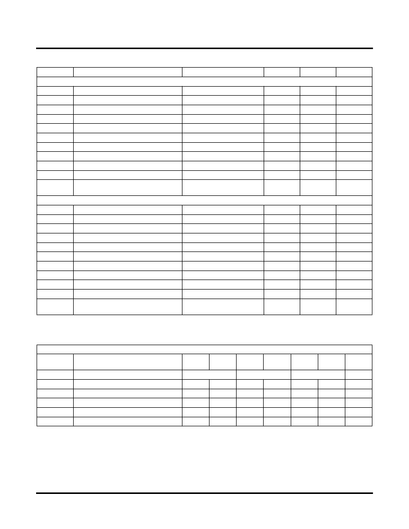
sysIO Differential Standards DC Electrical Characteristics
Parameter
LVDS
1
Description
Test Conditions
Min.
Typ.
Max.
V
INP,
V
INM
V
THD
V
CM
I
IN
V
OH
V
OL
V
OD
V
OD
V
OS
V
OS
I
OSD
Input voltage
0V
—
2.4V
Differential input threshold
+/-100mV
—
—
Input Common Mode voltage
Half the sum of the two inputs
0.05V
—
2.35V
Input current
Power on or Power off
—
—
+/-10uA
Output High Voltage for V
OP
or V
OM
Output Low Voltage for V
OP
or V
OM
Output Voltage Differential
RT = 100 Ohm
—
1.38V
1.60V
RT = 100 Ohm
0.9V
1.03V
—
|V
OP
- V
OM
|, R
T
= 100 ohm
250mV
350mV
450mV
Change in V
OD
between high and low
Output Voltage Offset
—
—
50mV
|V
OP
+ V
OM
|/2, R
T
= 100 ohm
1.125V
1.25V
1.375V
Change in V
OS
between H and L
Output short circuit current
—
—
50mV
V
OD
= 0V Driver outputs
shorted
—
—
24mA
BLVDS
1
V
INP,
V
INM
V
THD
V
CM
I
IN
V
OH
V
OL
V
OD
V
OD
V
OS
V
OS
I
OSD
Input voltage
0V
—
2.4V
Differential input threshold
+/-100mV
—
—
Input Common Mode voltage
Half the sum of the two inputs
0.05V
—
2.35V
Input current
Power on or Power off
—
—
+/-10uA
Output High Voltage for V
OP
or V
OM
Output Low Voltage for V
OP
or V
OM
Output Voltage Differential
R
T
= 27
R
T
= 27
|V
OP
- V
OM
|, RT = 27
—
1.4V
1.80V
0.95V
1.1V
—
240mV
300mV
460mV
Change in V
OD
Between H and L
Output Voltage Offset
27mV
|V
OP
+ V
OM
| /2, RT = 27
1.1V
1.3V
1.5V
Change in V
OS
Between H and L
Output Short Circuit Current
27mV
V
OD
= 0. Driver Outputs
Shorted.
36mA
65mA
1. V
OP
and V
OM
are the two outputs of the LVDS/BLVDS output buffer.
LVPECL
1
DC
Parameter
Parameter Description
Min.
Max.
Min.
Max.
Min.
Max.
Units
V
CCO
3.0
3.3
3.6
V
V
IH
V
IL
V
OH
V
OL
V
DIFF
1. These values are valid at the output of the source termination pack as shown above with 100-ohm differential load only (see Figure 22).
The V
OH
levels are 200mV below the standard LVPECL levels and are compatible with devices tolerant of the lower common mode ranges.
Input Voltage High
1.49
2.72
1.49
2.72
1.49
2.72
V
Input Voltage Low
0.86
2.125
0.86
2.125
0.86
2.125
V
Output Voltage High
1.8
2.11
1.92
2.28
2.13
2.41
V
Output Voltage Low
0.96
1.27
1.06
1.43
1.3
1.57
V
Differential Input voltage
0.3
—
0.3
—
0.3
—
V
相關(guān)PDF資料 |
PDF描述 |
|---|---|
| LFX200C-3F900C | The ispXPGA architecture |
| LFX200C-3F900I | The ispXPGA architecture |
| LFX500C-4F900I | The ispXPGA architecture |
| LFX1200C-03F900C | Circular Connector; MIL SPEC:MIL-C-26482, Series I; Body Material:Aluminum Alloy; Series:MS3112; No. of Contacts:19; Connector Shell Size:14; Connecting Termination:Solder; Circular Shell Style:Box Mount Receptacle RoHS Compliant: No |
| LFX1200C-03F900I | The ispXPGA architecture |
相關(guān)代理商/技術(shù)參數(shù) |
參數(shù)描述 |
|---|---|
| LFX1200B-03F900I | 制造商:LATTICE 制造商全稱:Lattice Semiconductor 功能描述:The ispXPGA architecture |
| LFX1200B-03FE680C | 功能描述:FPGA - 現(xiàn)場可編程門陣列 15376 LUT-4 496 I/O RoHS:否 制造商:Altera Corporation 系列:Cyclone V E 柵極數(shù)量: 邏輯塊數(shù)量:943 內(nèi)嵌式塊RAM - EBR:1956 kbit 輸入/輸出端數(shù)量:128 最大工作頻率:800 MHz 工作電源電壓:1.1 V 最大工作溫度:+ 70 C 安裝風(fēng)格:SMD/SMT 封裝 / 箱體:FBGA-256 |
| LFX1200B-03FEN680C | 功能描述:FPGA - 現(xiàn)場可編程門陣列 1.25M Gt ispJTAG 2. 5/3.3V -3 Spd RoHS:否 制造商:Altera Corporation 系列:Cyclone V E 柵極數(shù)量: 邏輯塊數(shù)量:943 內(nèi)嵌式塊RAM - EBR:1956 kbit 輸入/輸出端數(shù)量:128 最大工作頻率:800 MHz 工作電源電壓:1.1 V 最大工作溫度:+ 70 C 安裝風(fēng)格:SMD/SMT 封裝 / 箱體:FBGA-256 |
| LFX1200B-03FEN680C2 | 功能描述:FPGA - 現(xiàn)場可編程門陣列 15376 LUT-4 496 I/O RoHS:否 制造商:Altera Corporation 系列:Cyclone V E 柵極數(shù)量: 邏輯塊數(shù)量:943 內(nèi)嵌式塊RAM - EBR:1956 kbit 輸入/輸出端數(shù)量:128 最大工作頻率:800 MHz 工作電源電壓:1.1 V 最大工作溫度:+ 70 C 安裝風(fēng)格:SMD/SMT 封裝 / 箱體:FBGA-256 |
| LFX1200B-04F900C | 功能描述:FPGA - 現(xiàn)場可編程門陣列 15376 LUT-4 496 I/O RoHS:否 制造商:Altera Corporation 系列:Cyclone V E 柵極數(shù)量: 邏輯塊數(shù)量:943 內(nèi)嵌式塊RAM - EBR:1956 kbit 輸入/輸出端數(shù)量:128 最大工作頻率:800 MHz 工作電源電壓:1.1 V 最大工作溫度:+ 70 C 安裝風(fēng)格:SMD/SMT 封裝 / 箱體:FBGA-256 |
發(fā)布緊急采購,3分鐘左右您將得到回復(fù)。