- 您現(xiàn)在的位置:買賣IC網(wǎng) > PDF目錄377639 > LFX1200B-03F900C (LATTICE SEMICONDUCTOR CORP) The ispXPGA architecture PDF資料下載
參數(shù)資料
| 型號: | LFX1200B-03F900C |
| 廠商: | LATTICE SEMICONDUCTOR CORP |
| 元件分類: | FPGA |
| 英文描述: | The ispXPGA architecture |
| 中文描述: | FPGA, 3844 CLBS, 1250000 GATES, PBGA900 |
| 封裝: | FPBGA-900 |
| 文件頁數(shù): | 11/89頁 |
| 文件大小: | 941K |
| 代理商: | LFX1200B-03F900C |
第1頁第2頁第3頁第4頁第5頁第6頁第7頁第8頁第9頁第10頁當(dāng)前第11頁第12頁第13頁第14頁第15頁第16頁第17頁第18頁第19頁第20頁第21頁第22頁第23頁第24頁第25頁第26頁第27頁第28頁第29頁第30頁第31頁第32頁第33頁第34頁第35頁第36頁第37頁第38頁第39頁第40頁第41頁第42頁第43頁第44頁第45頁第46頁第47頁第48頁第49頁第50頁第51頁第52頁第53頁第54頁第55頁第56頁第57頁第58頁第59頁第60頁第61頁第62頁第63頁第64頁第65頁第66頁第67頁第68頁第69頁第70頁第71頁第72頁第73頁第74頁第75頁第76頁第77頁第78頁第79頁第80頁第81頁第82頁第83頁第84頁第85頁第86頁第87頁第88頁第89頁
Lattice Semiconductor
ispXPGA Family Data Sheet
11
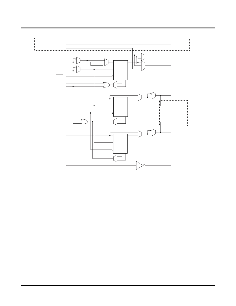
Figure 11. ispXPGA PIO
VLI Routing Resources
The ispXPGA architecture contains a Variable-Length-Interconnect (VLI) routing technology connecting the PFUs,
PICs, and EBRs in the device. There are four types of routing resources, Global Lines, Long Lines, General Inter-
connect, and Local Lines forming the global routing structure. This allows a signal to be routed to any element in
the device with the optimal delay.
The Global Lines consist of global clock lines and a global set/reset line. These lines are routed to all elements in
the device. They are speci
fi
cally designed for high speed, predictable timing regardless of fan-out. The global clock
lines can also be used as dedicated inputs.
The Long Lines consist of Horizontal and Vertical Long Lines (HLL and VLL). The VLL and HLL are tri-statable lines
spanning the entire device. These lines allow fast routing for high fan-out nets and general-purpose functions.
The General Interconnect consists of Double and Deca Lines. The Double Lines connect up to three elements (two
plus the driving element), while the Deca Lines connect up to eleven elements (ten plus the driving element).
The Local Lines are extremely fast routing paths consisting of Feedback and Direct Connect Lines. The Feedback
Lines are internal routing paths from the PFU outputs to the PFU inputs. The Direct Connect Lines connect all adja-
cent elements.
The Common Interface Block (CIB) provides the link between the logic element (PFU, PIC, or EBR) and the VLI
Routing resources. The CIB is a switch matrix that can be programmed to connect virtually any routing resource to
any input or output of the logic element.
Feed-through (FT)
OUT0
Clock (CLK)
Input Clock Enable (ICEN)
Input Set/Reset (ISR)
Global Set/Reset(GSR)
Output Clock Enable (OCEN)
PIO Input (IN)
Output Set/Reset (OSR)
PIO Output Enable(OEN)
PIO Input Enable (IEN)
OUT1
Delay
OE
From sysIO Input
To sysIO
Output
Enable
To sysIO
Output
CE
D
Q
S R
CLK/LE
CE
D
Q
S R
CLK/LE
CE
D
Q
S R
CLK/LE
From sysHSI block
From sysHSI block
To Routing
To sysHSI
block
To sysHSI
block
Only for PIOs associated with sysHSI Blocks
Only for PIOs
Associated with
sysHSI Blocks
相關(guān)PDF資料 |
PDF描述 |
|---|---|
| LFX200C-3F900C | The ispXPGA architecture |
| LFX200C-3F900I | The ispXPGA architecture |
| LFX500C-4F900I | The ispXPGA architecture |
| LFX1200C-03F900C | Circular Connector; MIL SPEC:MIL-C-26482, Series I; Body Material:Aluminum Alloy; Series:MS3112; No. of Contacts:19; Connector Shell Size:14; Connecting Termination:Solder; Circular Shell Style:Box Mount Receptacle RoHS Compliant: No |
| LFX1200C-03F900I | The ispXPGA architecture |
相關(guān)代理商/技術(shù)參數(shù) |
參數(shù)描述 |
|---|---|
| LFX1200B-03F900I | 制造商:LATTICE 制造商全稱:Lattice Semiconductor 功能描述:The ispXPGA architecture |
| LFX1200B-03FE680C | 功能描述:FPGA - 現(xiàn)場可編程門陣列 15376 LUT-4 496 I/O RoHS:否 制造商:Altera Corporation 系列:Cyclone V E 柵極數(shù)量: 邏輯塊數(shù)量:943 內(nèi)嵌式塊RAM - EBR:1956 kbit 輸入/輸出端數(shù)量:128 最大工作頻率:800 MHz 工作電源電壓:1.1 V 最大工作溫度:+ 70 C 安裝風(fēng)格:SMD/SMT 封裝 / 箱體:FBGA-256 |
| LFX1200B-03FEN680C | 功能描述:FPGA - 現(xiàn)場可編程門陣列 1.25M Gt ispJTAG 2. 5/3.3V -3 Spd RoHS:否 制造商:Altera Corporation 系列:Cyclone V E 柵極數(shù)量: 邏輯塊數(shù)量:943 內(nèi)嵌式塊RAM - EBR:1956 kbit 輸入/輸出端數(shù)量:128 最大工作頻率:800 MHz 工作電源電壓:1.1 V 最大工作溫度:+ 70 C 安裝風(fēng)格:SMD/SMT 封裝 / 箱體:FBGA-256 |
| LFX1200B-03FEN680C2 | 功能描述:FPGA - 現(xiàn)場可編程門陣列 15376 LUT-4 496 I/O RoHS:否 制造商:Altera Corporation 系列:Cyclone V E 柵極數(shù)量: 邏輯塊數(shù)量:943 內(nèi)嵌式塊RAM - EBR:1956 kbit 輸入/輸出端數(shù)量:128 最大工作頻率:800 MHz 工作電源電壓:1.1 V 最大工作溫度:+ 70 C 安裝風(fēng)格:SMD/SMT 封裝 / 箱體:FBGA-256 |
| LFX1200B-04F900C | 功能描述:FPGA - 現(xiàn)場可編程門陣列 15376 LUT-4 496 I/O RoHS:否 制造商:Altera Corporation 系列:Cyclone V E 柵極數(shù)量: 邏輯塊數(shù)量:943 內(nèi)嵌式塊RAM - EBR:1956 kbit 輸入/輸出端數(shù)量:128 最大工作頻率:800 MHz 工作電源電壓:1.1 V 最大工作溫度:+ 70 C 安裝風(fēng)格:SMD/SMT 封裝 / 箱體:FBGA-256 |
發(fā)布緊急采購,3分鐘左右您將得到回復(fù)。