- 您現(xiàn)在的位置:買賣IC網(wǎng) > PDF目錄377639 > LFX1200B-03F900C (LATTICE SEMICONDUCTOR CORP) The ispXPGA architecture PDF資料下載
參數(shù)資料
| 型號: | LFX1200B-03F900C |
| 廠商: | LATTICE SEMICONDUCTOR CORP |
| 元件分類: | FPGA |
| 英文描述: | The ispXPGA architecture |
| 中文描述: | FPGA, 3844 CLBS, 1250000 GATES, PBGA900 |
| 封裝: | FPBGA-900 |
| 文件頁數(shù): | 16/89頁 |
| 文件大小: | 941K |
| 代理商: | LFX1200B-03F900C |
第1頁第2頁第3頁第4頁第5頁第6頁第7頁第8頁第9頁第10頁第11頁第12頁第13頁第14頁第15頁當(dāng)前第16頁第17頁第18頁第19頁第20頁第21頁第22頁第23頁第24頁第25頁第26頁第27頁第28頁第29頁第30頁第31頁第32頁第33頁第34頁第35頁第36頁第37頁第38頁第39頁第40頁第41頁第42頁第43頁第44頁第45頁第46頁第47頁第48頁第49頁第50頁第51頁第52頁第53頁第54頁第55頁第56頁第57頁第58頁第59頁第60頁第61頁第62頁第63頁第64頁第65頁第66頁第67頁第68頁第69頁第70頁第71頁第72頁第73頁第74頁第75頁第76頁第77頁第78頁第79頁第80頁第81頁第82頁第83頁第84頁第85頁第86頁第87頁第88頁第89頁
Lattice Semiconductor
ispXPGA Family Data Sheet
16
The second type of interface implemented is the terminated, single-ended interface standard. This group of inter-
faces includes different versions of SSTL and HSTL interfaces along with CTT, and GTL+. Usage of these particu-
lar I/O interfaces requires an additional V
REF
signal. At the system level a termination voltage, V
Typically an output will be terminated to V
TT
at the receiving end of the transmission line it is driving.
TT
, is also required.
The third type of interface standards are the differential standards LVDS, BLVDS, and LVPECL. The differential
standards require two I/O pins to create the differential pair. The logic level is determined by the difference in the
two signals. Table 6 lists how these interface standards are implemented in the ispXPGA devices.
For more information on sysIO capability, refer to Lattice technical note number TN1000,
for Lattice Devices
available at www.latticesemi.com.
sysIO Usage Guidelines
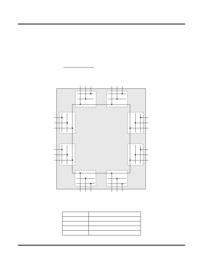
Figure 19. sysIO Banks per Device
Table 4. Number of I/Os per Bank
Device
Max. Number of I/Os per Bank (N)
XPGA 1200
62
XPGA 500
42
XPGA 200
26
XPGA 125
22
GND
V
CCO0
V
REF0
GND
V
CCO1
V
REF1
GND
V
CCO5
V
REF5
GND
V
CCO4
V
REF4
G
V
C
V
R
G
V
C
V
R
G
V
C
V
R
G
I
I
I/O 0
I/O 0
I/O N
I/O N
I/O N
I/O N
I/O 0
I/O 0
I
I
I
I
I
I
V
C
V
R
Bank 3
Bank 2
Bank 6
Bank 7
B
B
B
B
相關(guān)PDF資料 |
PDF描述 |
|---|---|
| LFX200C-3F900C | The ispXPGA architecture |
| LFX200C-3F900I | The ispXPGA architecture |
| LFX500C-4F900I | The ispXPGA architecture |
| LFX1200C-03F900C | Circular Connector; MIL SPEC:MIL-C-26482, Series I; Body Material:Aluminum Alloy; Series:MS3112; No. of Contacts:19; Connector Shell Size:14; Connecting Termination:Solder; Circular Shell Style:Box Mount Receptacle RoHS Compliant: No |
| LFX1200C-03F900I | The ispXPGA architecture |
相關(guān)代理商/技術(shù)參數(shù) |
參數(shù)描述 |
|---|---|
| LFX1200B-03F900I | 制造商:LATTICE 制造商全稱:Lattice Semiconductor 功能描述:The ispXPGA architecture |
| LFX1200B-03FE680C | 功能描述:FPGA - 現(xiàn)場可編程門陣列 15376 LUT-4 496 I/O RoHS:否 制造商:Altera Corporation 系列:Cyclone V E 柵極數(shù)量: 邏輯塊數(shù)量:943 內(nèi)嵌式塊RAM - EBR:1956 kbit 輸入/輸出端數(shù)量:128 最大工作頻率:800 MHz 工作電源電壓:1.1 V 最大工作溫度:+ 70 C 安裝風(fēng)格:SMD/SMT 封裝 / 箱體:FBGA-256 |
| LFX1200B-03FEN680C | 功能描述:FPGA - 現(xiàn)場可編程門陣列 1.25M Gt ispJTAG 2. 5/3.3V -3 Spd RoHS:否 制造商:Altera Corporation 系列:Cyclone V E 柵極數(shù)量: 邏輯塊數(shù)量:943 內(nèi)嵌式塊RAM - EBR:1956 kbit 輸入/輸出端數(shù)量:128 最大工作頻率:800 MHz 工作電源電壓:1.1 V 最大工作溫度:+ 70 C 安裝風(fēng)格:SMD/SMT 封裝 / 箱體:FBGA-256 |
| LFX1200B-03FEN680C2 | 功能描述:FPGA - 現(xiàn)場可編程門陣列 15376 LUT-4 496 I/O RoHS:否 制造商:Altera Corporation 系列:Cyclone V E 柵極數(shù)量: 邏輯塊數(shù)量:943 內(nèi)嵌式塊RAM - EBR:1956 kbit 輸入/輸出端數(shù)量:128 最大工作頻率:800 MHz 工作電源電壓:1.1 V 最大工作溫度:+ 70 C 安裝風(fēng)格:SMD/SMT 封裝 / 箱體:FBGA-256 |
| LFX1200B-04F900C | 功能描述:FPGA - 現(xiàn)場可編程門陣列 15376 LUT-4 496 I/O RoHS:否 制造商:Altera Corporation 系列:Cyclone V E 柵極數(shù)量: 邏輯塊數(shù)量:943 內(nèi)嵌式塊RAM - EBR:1956 kbit 輸入/輸出端數(shù)量:128 最大工作頻率:800 MHz 工作電源電壓:1.1 V 最大工作溫度:+ 70 C 安裝風(fēng)格:SMD/SMT 封裝 / 箱體:FBGA-256 |
發(fā)布緊急采購,3分鐘左右您將得到回復(fù)。