- 您現在的位置:買賣IC網 > PDF目錄383236 > L6260 (意法半導體) 4.5 - 5.5V DISK DRIVER SPINDLE & VCM, POWER & CONTROL COMBO’S PDF資料下載
參數資料
| 型號: | L6260 |
| 廠商: | 意法半導體 |
| 英文描述: | 4.5 - 5.5V DISK DRIVER SPINDLE & VCM, POWER & CONTROL COMBO’S |
| 中文描述: | 4.5 - 5.5V的磁盤驅動程序主軸 |
| 文件頁數: | 17/30頁 |
| 文件大小: | 305K |
| 代理商: | L6260 |
第1頁第2頁第3頁第4頁第5頁第6頁第7頁第8頁第9頁第10頁第11頁第12頁第13頁第14頁第15頁第16頁當前第17頁第18頁第19頁第20頁第21頁第22頁第23頁第24頁第25頁第26頁第27頁第28頁第29頁第30頁
The duration of the brake delay is defined by an
external resistor and capacitor connected to the
brake delay pin (BRK_DLY). Charge stored in an
external capacitor connected to the Voltage Tri-
pler (VPDOWN) is used to supply the brake delay
circuit after the loss of power.
During the application of power to the IC, the
power on reset signal (POR) is asserted, forcing
all registers to their default state (see @POR col-
umn of the register definitions) and disabling the
VCM and spindle drivers. Once the supply volt-
age has exceeded the Voltage Good (VGT)
threshold,the POR delay begins.When this delay
has expired, POR is de-asserted. It is this delay
whose duration is determined by an external ca-
pacitor connectedto the POR_D
LY
pin.
When a low voltage condition is detected (the
supply voltage falls below the VGT) the following
happens (in order):
1)
Internal registers are reset and POR is as-
serted.
2) The automatic parking of the actuator is en-
abledand the brake delay starts.
3) After the brake delay expires,all lowside driv-
ers are enabled to brake the spindle.
SerialInterface
The serial interface is designed to be compatible
with the Intel 80196 (and other similar micros) se-
rial interface but is capable of faster data rates,
up to 10 MHz. All read and write operationsmust
consist of 16 bits, with the 80196 this would be
two 8 bit accesses. The first four bits are address
and the next 12 are data. If the address is a read
register then the L6260 will use the SCLK from
the system to shift out 12 bits of data from the ad-
dressed register. The system must provide 16
SCLK pulses to insure that the read operation
completes.
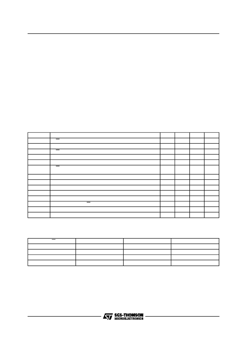
SYMBOL
t
RWS
t
SLS
t
RWH
t
SLH
t
SCKD
t
RWD
DESCRIPTION
MIN.
100
100
100
100
TYP.
MAX.
UNITS
ns
ns
ns
ns
ns
ns
R/W setup time to SCLK going high
SLOAD setup time to SCLK going high
R/W hold time after SCLK going high
SLOAD hold time after SCLK going high
SCLK high to Data Valid
R/W High to Data Valid
Data bit D[0] valid from HiZ
Address setup time to SCLK going high
Data setup time to SCLK going High
Address Hold after SCLK going high
Data Hold time after SCLK going High
SDIO tri-state after SLOAD going High
SDIO tri-state after R/W going low
Minimum SCLK period
Recycle - Time between successive accesses
30
30
50
50
t
AS
t
DS
t
AH
t
DH
t
SDZ
t
RWZ
t
PER
t
REC
(*)
30
30
10
10
30
30
100
100
ns
ns
ns
ns
ns
ns
ns
ns
(*) For 10MHz system clock operation (in other words. 1 or more clock cycles of SCLK).
Serial InterfaceTruthTable
R/
W
1
0
0
1
SLOAD
1
1
0
0
SDIO
DIRECTION
Tri-state
Tri-state
Input
Output
Tri-state (Port unselected)
Tri-state (Port unselected)
Address/Data input
Data output
L6260
17/30
相關PDF資料 |
PDF描述 |
|---|---|
| L6268 | 12V DISK DRIVE SPINDLE & VCM, POWER & CONTROL “COMBO” |
| L6269 | 12V DISK DRIVE SPINDLE & VCM, POWER & CONTROL “COMBO” |
| L6270 | MILLI-ACTUATOR DRIVER |
| L6271 | MILLI-ACTUATOR DRIVER |
| L6275 | 5V DISK DRIVE SPINDLE & VCM, POWER & CONTROL “COMBO” |
相關代理商/技術參數 |
參數描述 |
|---|---|
| L6261 | 制造商:未知廠家 制造商全稱:未知廠家 功能描述:Servo/Spindle Motor Controller/Driver |
| L62622.6 | 制造商:STMicroelectronics 功能描述: |
| L6268 | 制造商:STMICROELECTRONICS 制造商全稱:STMicroelectronics 功能描述:12V DISK DRIVE SPINDLE & VCM, POWER & CONTROL “COMBO” |
| L6269 | 制造商:STMicroelectronics 功能描述:L6269 - Trays |
| L6269TR | 制造商:STMicroelectronics 功能描述:12V SMART POWER COMBO - Tape and Reel |
發(fā)布緊急采購,3分鐘左右您將得到回復。