- 您現(xiàn)在的位置:買賣IC網(wǎng) > PDF目錄374352 > KM29N16000ATS (SAMSUNG SEMICONDUCTOR CO. LTD.) 2M x 8 Bit NAND Flash Memory(2M x 8位 NAND閃速存儲器) PDF資料下載
參數(shù)資料
| 型號: | KM29N16000ATS |
| 廠商: | SAMSUNG SEMICONDUCTOR CO. LTD. |
| 英文描述: | 2M x 8 Bit NAND Flash Memory(2M x 8位 NAND閃速存儲器) |
| 中文描述: | 200萬× 8位NAND閃存(2米× 8位的NAND閃速存儲器) |
| 文件頁數(shù): | 17/21頁 |
| 文件大小: | 252K |
| 代理商: | KM29N16000ATS |
KM29N16000ATS
FLASH MEMORY
17
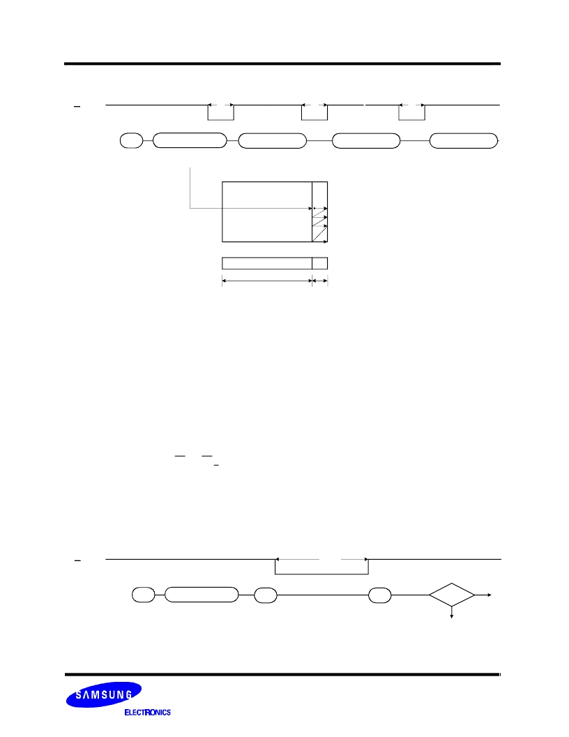
Figure 6. Sequential Row Read2 Operation
PAGE PROGRAM
The device is programmed basically on a page basis. But it also allows multiple partial page programming of a byte or consecutiv e
bytes up to 264 may be programmed in a single page program cycle. The number of partial page programming operation in the same
page without an intervening erase operation must not exceed ten. The addressing may be done in random order in a block. A page
program cycle consist of a serial data loading period in which up to 264 bytes of data must be loaded into the device, and nonvo latile
programming period in which the loaded data is programmed into the appropriate cell.
The sequential data loading period begins by inputting the Serial Data Input command(80H), followed by the three cycle address
input and then serial data loading. The bytes other than those to be programmed do not need to be loaded.
In order to program the bytes in the spare columns of 256 to 263, the pointer should be set to the spare area by writing the Rea d 2
command(50H) to the command register. The pointer remains in the spare area unless the Read 1 command(00H) is entered to
retum to the main area. The Page Program confirm command(10H) initiates the programming process. Writing 10H alone without
perviously entering the serial data will not initiate the programming process. The internal write controller automatically execu tes the
algorithms and timings necessary for program and verify, thereby freeing the CPU for other tasks. Once the program process start s,
the Status Register may be read RE and CE low after the Read Status command(70H) is written to it. The CPU can detect the com-
pletion of program cycle by monitoring the R/ B output, or the Status bit(I/O
6
) of the Status Register. Only the Read Status command
and Reset command are valid while programming is in progress. When the Page Program is complete, the Write Status Bit(I/O
be checked(Figure 7). The internal write verify detects only errors for "1"s that are not successfully programmed to "0"s. The c om-
mand register remains in Read Status command mode until another valid command is written to the command register.
0
) may
50H
A
0
~ A
2
& A
8
~ A
20
I/O
0
~
7
R/B
Start Add.(3Cycle)
Data Output
Data Output
Data Output
2nd
(8Byte)
Nth
(8Byte)
Data Field
Spare Field
1st
2nd
Nth
(A
3
~ A
7
:
Don't Care)
1st
Figure 7. Program & Read Status Operation
80H
A
0
~ A
7
& A
8
~ A
20
264 Byte Data
I/O
0 ~ 7
R/B
Address & Data Input
I/O
0
Pass
10H
70H
Fail
t
R
t
R
t
R
t
PROG
≈
相關(guān)PDF資料 |
PDF描述 |
|---|---|
| KM29N32000IT | 4M x 8 Bit NAND Flash Memory(4M x 8位 NAND閃速存儲器) |
| KM29N32000T | 4M x 8 Bit NAND Flash Memory(4M x 8位 NAND閃速存儲器) |
| KM29N32000TS | 4M x 8 Bit NAND Flash Memory(4M x 8位 NAND閃速存儲器) |
| KM29U128IT | 16M x 8 Bit NAND Flash Memory |
| KM29U128T | 16M x 8 Bit NAND Flash Memory |
相關(guān)代理商/技術(shù)參數(shù) |
參數(shù)描述 |
|---|---|
| KM29U128IT | 制造商:SAMSUNG 制造商全稱:Samsung semiconductor 功能描述:16M x 8 Bit NAND Flash Memory |
| KM29U128T | 制造商:SAMSUNG 制造商全稱:Samsung semiconductor 功能描述:16M x 8 Bit NAND Flash Memory |
| KM29U64000IT | 制造商:SAMSUNG 制造商全稱:Samsung semiconductor 功能描述:8M x 8 Bit NAND Flash Memory |
| KM29U64000T | 制造商:SAMSUNG 制造商全稱:Samsung semiconductor 功能描述:8M x 8 Bit NAND Flash Memory |
| KM29V16000AIT | 制造商:SAMSUNG 制造商全稱:Samsung semiconductor 功能描述:FLASH MEMORY |
發(fā)布緊急采購,3分鐘左右您將得到回復(fù)。