- 您現(xiàn)在的位置:買(mǎi)賣(mài)IC網(wǎng) > PDF目錄223865 > GS8321E18AD-333IT (GSI TECHNOLOGY) CACHE SRAM, PBGA165 PDF資料下載
參數(shù)資料
| 型號(hào): | GS8321E18AD-333IT |
| 廠商: | GSI TECHNOLOGY |
| 元件分類: | SRAM |
| 英文描述: | CACHE SRAM, PBGA165 |
| 封裝: | FPBGA-165 |
| 文件頁(yè)數(shù): | 30/32頁(yè) |
| 文件大小: | 736K |
| 代理商: | GS8321E18AD-333IT |
第1頁(yè)第2頁(yè)第3頁(yè)第4頁(yè)第5頁(yè)第6頁(yè)第7頁(yè)第8頁(yè)第9頁(yè)第10頁(yè)第11頁(yè)第12頁(yè)第13頁(yè)第14頁(yè)第15頁(yè)第16頁(yè)第17頁(yè)第18頁(yè)第19頁(yè)第20頁(yè)第21頁(yè)第22頁(yè)第23頁(yè)第24頁(yè)第25頁(yè)第26頁(yè)第27頁(yè)第28頁(yè)第29頁(yè)當(dāng)前第30頁(yè)第31頁(yè)第32頁(yè)
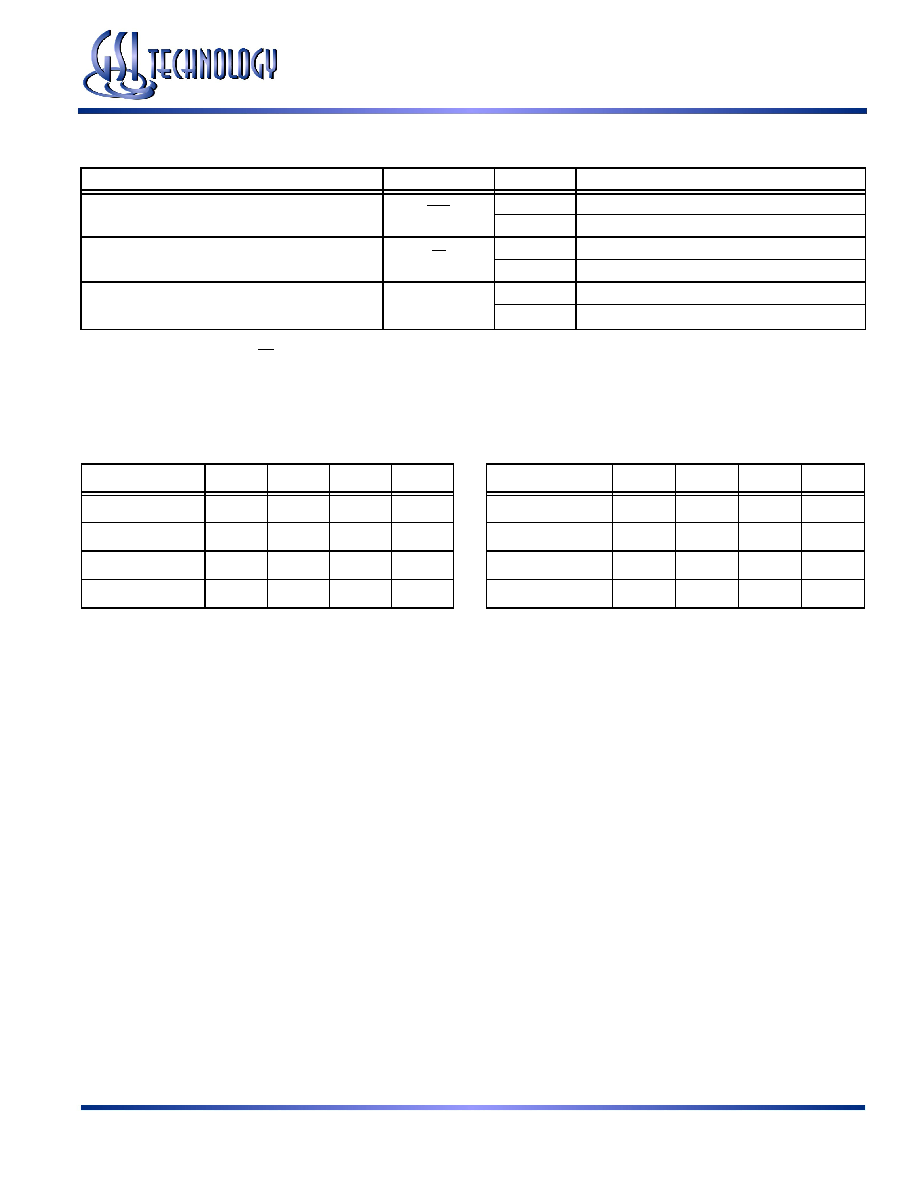
Mode Pin Functions
Mode Name
Pin Name
State
Function
Burst Order Control
LBO
L
Linear Burst
H
Interleaved Burst
Output Register Control
FT
L
Flow Through
H or NC
Pipeline
Power Down Control
ZZ
L or NC
Active
H
Standby, IDD = ISB
GS8321E18/32/36AD-400/375/333/250/200/150
Specifications cited are subject to change without notice. For latest documentation see http://www.gsitechnology.com.
Rev: 1.00a 2/2011
7/32
2010, GSI Technology
Preliminary
Note:
There is a pull-up device on the FT pin and a pull-down device on the ZZ pin , so this input pin can be unconnected and the chip will operate in
the default states as specified in the above tables.
Note:
The burst counter wraps to initial state on the 5th clock.
Note:
The burst counter wraps to initial state on the 5th clock.
Linear Burst Sequence
A[1:0]
1st address
00
01
10
11
2nd address
01
10
11
00
3rd address
10
11
00
01
4th address
11
00
01
10
Interleaved Burst Sequence
A[1:0]
1st address
00
01
10
11
2nd address
01
00
11
10
3rd address
10
11
00
01
4th address
11
10
01
00
Burst Counter Sequences
相關(guān)PDF資料 |
PDF描述 |
|---|---|
| GS832236AB-150VT | 1M X 36 CACHE SRAM, 7.5 ns, PBGA119 |
| GS8342D11BD-500IT | 4M X 9 QDR SRAM, 0.45 ns, PBGA165 |
| GS8342D11BD-500 | 4M X 9 QDR SRAM, 0.45 ns, PBGA165 |
| GS8342D11BD-550IT | 4M X 9 QDR SRAM, 0.45 ns, PBGA165 |
| GS8342D37BD-300I | 1M X 36 QDR SRAM, 0.45 ns, PBGA165 |
相關(guān)代理商/技術(shù)參數(shù) |
參數(shù)描述 |
|---|---|
| GS8321E18AD-375 | 制造商:GSI Technology 功能描述:165 BGA - Bulk |
| GS8321E18AGD-375 | 制造商:GSI Technology 功能描述:165 FPBGA - Bulk |
| GS8321E18AGD-375I | 制造商:GSI Technology 功能描述:165 FPBGA - Bulk |
| GS8321E18E | 制造商:GSI 制造商全稱:GSI Technology 功能描述:2M x 18, 1M x 32, 1M x 36 36Mb Sync Burst SRAMs |
| GS8321E18E-133 | 制造商:GSI 制造商全稱:GSI Technology 功能描述:2M x 18, 1M x 32, 1M x 36 36Mb Sync Burst SRAMs |
發(fā)布緊急采購(gòu),3分鐘左右您將得到回復(fù)。