- 您現(xiàn)在的位置:買賣IC網(wǎng) > PDF目錄379098 > CYD04S36V (Cypress Semiconductor Corp.) FLEx36TM 3.3V 32K/64K/128K/256K/512 x 36 Synchronous Dual-Port RAM(FLEx36TM 3.3V 32K/64K/128K/256K/512 x 36同步雙端口RAM) PDF資料下載
參數(shù)資料
| 型號: | CYD04S36V |
| 廠商: | Cypress Semiconductor Corp. |
| 英文描述: | FLEx36TM 3.3V 32K/64K/128K/256K/512 x 36 Synchronous Dual-Port RAM(FLEx36TM 3.3V 32K/64K/128K/256K/512 x 36同步雙端口RAM) |
| 中文描述: | FLEx36TM 3.3 32K/64K/128K/256K/512 × 36同步雙口RAM(FLEx36TM 3.3 32K/64K/128K/256K/512 × 36同步雙端口RAM)的 |
| 文件頁數(shù): | 12/28頁 |
| 文件大?。?/td> | 608K |
| 代理商: | CYD04S36V |
第1頁第2頁第3頁第4頁第5頁第6頁第7頁第8頁第9頁第10頁第11頁當(dāng)前第12頁第13頁第14頁第15頁第16頁第17頁第18頁第19頁第20頁第21頁第22頁第23頁第24頁第25頁第26頁第27頁第28頁
CYD01S36V
CYD02S36V/CYD04S36V
CYD09S36V/CYD18S36V
Document #: 38-06076 Rev. *E
Page 12 of 28
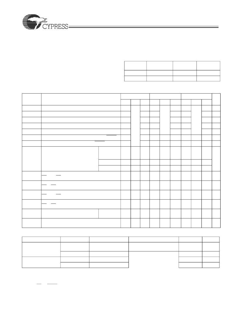
Maximum Ratings
[25]
(Above which the useful life may be impaired. For user guide-
lines, not tested.)
Storage Temperature ..................................–65°C to +150°C
Ambient Temperature with
Power Applied.............................................–55°C to +125°C
Supply Voltage to Ground Potential...............–0.5V to +4.6V
DC Voltage Applied to
Outputs in High-Z State...........................–0.5V to V
DD
+0.5V
DC Input Voltage...............................–0.5V to V
DD
+ 0.5V
[26]
Electrical Characteristics
Over the Operating Range
Output Current into Outputs (LOW).............................20 mA
Static Discharge Voltage...........................................> 2000V
(JEDEC JESD22-A114-2000B)
Latch-up Current.....................................................> 200 mA
Operating Range
Range
Commercial
Industrial
Ambient
Temperature
0°C to +70°C 3.3V±165 mV 1.8V±100 mV
–40°C to +85°C 3.3V±165 mV 1.8V±100 mV
V
DDIO/VTTL
V
CORE
[13]
Parameter
V
OH
V
OL
V
IH
V
IL
I
OZ
I
IX1
I
IX2
I
CC
Description
-167
-133
Typ.
-100
Typ. Max.
Unit
V
V
V
V
μ
A
μ
A
mA
mA
Min. Typ. Max. Min.
2.4
Max. Min.
Output HIGH Voltage (V
DD
= Min., I
OH
= –4.0 mA)
Output LOW Voltage (V
DD
= Min., I
OL
= +4.0 mA)
Input HIGH Voltage
Input LOW Voltage
Output Leakage Current
Input Leakage Current Except TDI, TMS, MRST
Input Leakage Current TDI, TMS, MRST
Operating Current for
(V
= Max.,I
OUT
= 0 mA), Outputs
Disabled
2.4
2.4
0.4
0.4
0.4
2.0
2.0
2.0
0.8
10
10
0.1
300
0.8
10
10
0.1
300
0.8
10
10
0.1
–10
–10
–1.0
–10
–10
–1.0
–10
–10
–1.0
CYD01S36V
CYD02S36V/
CYD04S36V
CYD09S36V
CYD18S36V
225
225
450
600
370
410
90
540
580
115
315
450
I
SB1[27]
Standby Current (Both Ports TTL Level)
CE
L
and CE
R
≥
V
IH
, f = f
MAX
Standby Current (One Port TTL Level)
CE
L
| CE
R
≥
V
IH
, f = f
MAX
Standby Current (Both Ports CMOS Level)
CE
L
and CE
R
≥
V
DD
– 0.2V, f = 0
Standby Current (One Port CMOS Level)
CE
L
| CE
R
≥
V
IH
, f = f
MAX
Operating Current (VDDIO = Max,
Iout = 0 mA, f = 0) Outputs Disabled
Core Operating Current for (V
DD
= Max., I
OUT
= 0
mA), Outputs Disabled
90
115
mA
I
SB2[27]
160
210
160
210
mA
I
SB3[27]
55
75
55
75
mA
I
SB4[27]
160
210
160
210
mA
I
SB5
CYD18S36V
75
75
mA
I
CORE[13]
0
0
0
0
0
0
mA
Capacitance
[28]
Part Number
CYD01S36/
CYD02S36V/
CYD04S36V
Parameter
C
IN
Description
Input Capacitance
Test Conditions
T
A
= 25°C, f = 1 MHz,
V
DD
= 3.3V
Max.
13
Unit
pF
C
OUT
C
IN
C
OUT
Output Capacitance
Input Capacitance
Output Capacitance
10
22
pF
pF
pF
CYD09S36V
10
[29]
Notes:
25.The voltage on any input or I/O pin can not exceed the power pin during power-up.
26.Pulse width < 20 ns.
27.I
SB1
, I
, I
and I
are not applicable for CYD18S36V because it cannot be powered down by using chip enable pins.
28.C
also references C
.
29.Except INT and CNTINT which are 20 pF.
相關(guān)PDF資料 |
PDF描述 |
|---|---|
| CYD09S36V | FLEx36TM 3.3V 32K/64K/128K/256K/512 x 36 Synchronous Dual-Port RAM(FLEx36TM 3.3V 32K/64K/128K/256K/512 x 36同步雙端口RAM) |
| CYD18S72V18 | FullFlex Synchronous SDR Dual-Port SRAM(FullFlex同步SDR雙端口SRAM) |
| CYD04S72V18 | FullFlex Synchronous SDR Dual-Port SRAM(FullFlex同步SDR雙端口SRAM) |
| CYD36S72V18 | FullFlex Synchronous SDR Dual-Port SRAM(FullFlex同步SDR雙端口SRAM) |
| CYD09S72V18 | FullFlex Synchronous SDR Dual-Port SRAM(FullFlex同步SDR雙端口SRAM) |
相關(guān)代理商/技術(shù)參數(shù) |
參數(shù)描述 |
|---|---|
| CYD04S36V-133BBC | 制造商:Cypress Semiconductor 功能描述: |
| CYD04S36V-133BBI | 制造商:Cypress Semiconductor 功能描述: |
| CYD04S36V-167BBC | 制造商:Cypress Semiconductor 功能描述: |
| CYD04S36V18 | 制造商:CYPRESS 制造商全稱:Cypress Semiconductor 功能描述:18-Mb/9-Mb/4-Mb x36/x18 FullFlex⑩ Dual-Ports |
| CYD04S36V18-167BBXC | 功能描述:靜態(tài)隨機存取存儲器 4M Sync Dual Port 128Kx36 90nm COM RoHS:否 制造商:Cypress Semiconductor 存儲容量:16 Mbit 組織:1 M x 16 訪問時間:55 ns 電源電壓-最大:3.6 V 電源電壓-最小:2.2 V 最大工作電流:22 uA 最大工作溫度:+ 85 C 最小工作溫度:- 40 C 安裝風(fēng)格:SMD/SMT 封裝 / 箱體:TSOP-48 封裝:Tray |
發(fā)布緊急采購,3分鐘左右您將得到回復(fù)。