- 您現(xiàn)在的位置:買賣IC網(wǎng) > PDF目錄379077 > CY7C1471V33-133BZXC (CYPRESS SEMICONDUCTOR CORP) 72-Mbit (2M x 36/4M x 18/1M x 72) Flow-Through SRAM with NoBL Architecture PDF資料下載
參數(shù)資料
| 型號: | CY7C1471V33-133BZXC |
| 廠商: | CYPRESS SEMICONDUCTOR CORP |
| 元件分類: | DRAM |
| 英文描述: | 72-Mbit (2M x 36/4M x 18/1M x 72) Flow-Through SRAM with NoBL Architecture |
| 中文描述: | 2M X 36 ZBT SRAM, 6.5 ns, PBGA165 |
| 封裝: | 15 X 17 MM, 1.40 MM HEIGHT, LEAD FREE, FBGA-165 |
| 文件頁數(shù): | 14/29頁 |
| 文件大?。?/td> | 375K |
| 代理商: | CY7C1471V33-133BZXC |
第1頁第2頁第3頁第4頁第5頁第6頁第7頁第8頁第9頁第10頁第11頁第12頁第13頁當前第14頁第15頁第16頁第17頁第18頁第19頁第20頁第21頁第22頁第23頁第24頁第25頁第26頁第27頁第28頁第29頁
PRELIMINARY
CY7C1471V33
CY7C1473V33
CY7C1475V33
Document #: 38-05288 Rev. *E
Page 14 of 29
possible to capture all other signals and simply ignore the
value of the CLK captured in the boundary scan register.
Once the data is captured, it is possible to shift out the data by
putting the TAP into the Shift-DR state. This places the
boundary scan register between the TDI and TDO balls.
Note that since the PRELOAD part of the command is not
implemented, putting the TAP to the Update-DR state while
performing a SAMPLE/PRELOAD instruction will have the
same effect as the Pause-DR command.
BYPASS
When the BYPASS instruction is loaded in the instruction
register and the TAP is placed in a Shift-DR state, the bypass
register is placed between the TDI and TDO balls. The
advantage of the BYPASS instruction is that it shortens the
boundary scan path when multiple devices are connected
together on a board.
Reserved
These instructions are not implemented but are reserved for
future use. Do not use these instructions.
TAP Timing
TAP AC Switching Characteristics
Over the Operating Range
[10, 11]
Parameter
Clock
t
TCYC
t
TF
t
TH
t
TL
Output Times
t
TDOV
t
TDOX
Set-up Times
t
TMSS
t
TDIS
t
CS
Hold Times
t
TMSH
t
TDIH
t
CH
Notes:
10.t
and t
refer to the set-up and hold time requirements of latching data from the boundary scan register.
11.Test conditions are specified using the load in TAP AC test Conditions. t
R
/t
F
= 1 ns.
Description
Min.
Max
Unit
TCK Clock Cycle Time
TCK Clock Frequency
TCK Clock HIGH time
TCK Clock LOW time
50
ns
MHz
ns
ns
20
25
25
TCK Clock LOW to TDO Valid
TCK Clock LOW to TDO Invalid
5
ns
ns
0
TMS Set-up to TCK Clock Rise
TDI Set-up to TCK Clock Rise
Capture Set-up to TCK Rise
5
5
5
ns
ns
ns
TMS hold after TCK Clock Rise
TDI Hold after Clock Rise
Capture Hold after Clock Rise
5
5
5
ns
ns
ns
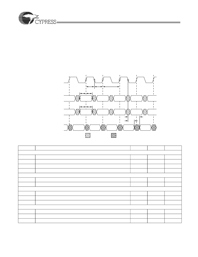
tTL
Test Clock
(TCK)
1
2
3
4
5
6
Test Mode Select
(TMS)
tTH
Test Data-Out
(TDO)
tCYC
Test Data-In
(TDI)
tTMSH
tTMSS
tTDIH
tTDIS
tTDOX
tTDOV
DON’T CARE
UNDEFINED
相關PDF資料 |
PDF描述 |
|---|---|
| CY7C1471V33-100AXC | 72-Mbit (2M x 36/4M x 18/1M x 72) Flow-Through SRAM with NoBL Architecture |
| CY7C1474V33-250BGI | 72-Mbit (2M x 36/4M x 18/1M x 72) Pipelined SRAM with NoBL⑩ Architecture |
| CY7C1474V33-250BGXI | 72-Mbit (2M x 36/4M x 18/1M x 72) Pipelined SRAM with NoBL⑩ Architecture |
| CY7C1475V25-100BGI | 72-Mbit (2M x 36/4M x 18/1M x 72) Flow-Through SRAM with NoBL⑩ Architecture |
| CY7C1475V25-100BGXI | 72-Mbit (2M x 36/4M x 18/1M x 72) Flow-Through SRAM with NoBL⑩ Architecture |
相關代理商/技術參數(shù) |
參數(shù)描述 |
|---|---|
| CY7C1471XC | 制造商:Cypress Semiconductor 功能描述: |
| CY7C14722AC | 制造商:Cypress Semiconductor 功能描述: |
| CY7C14722BC | 制造商:Cypress Semiconductor 功能描述: |
| CY7C1472BC | 制造商:Cypress Semiconductor 功能描述: |
| CY7C1472BV25-200AXC | 功能描述:靜態(tài)隨機存取存儲器 72MB (4Mx18) 2.5v 200MHz 靜態(tài)隨機存取存儲器 RoHS:否 制造商:Cypress Semiconductor 存儲容量:16 Mbit 組織:1 M x 16 訪問時間:55 ns 電源電壓-最大:3.6 V 電源電壓-最小:2.2 V 最大工作電流:22 uA 最大工作溫度:+ 85 C 最小工作溫度:- 40 C 安裝風格:SMD/SMT 封裝 / 箱體:TSOP-48 封裝:Tray |
發(fā)布緊急采購,3分鐘左右您將得到回復。