- 您現(xiàn)在的位置:買賣IC網(wǎng) > PDF目錄379006 > CY2833 (Cypress Semiconductor Corp.) Intel CK408 Mobile Clock Synthesizer PDF資料下載
參數(shù)資料
| 型號(hào): | CY2833 |
| 廠商: | Cypress Semiconductor Corp. |
| 英文描述: | Intel CK408 Mobile Clock Synthesizer |
| 中文描述: | 英特爾CK408移動(dòng)時(shí)鐘合成器 |
| 文件頁(yè)數(shù): | 9/18頁(yè) |
| 文件大小: | 224K |
| 代理商: | CY2833 |
第1頁(yè)第2頁(yè)第3頁(yè)第4頁(yè)第5頁(yè)第6頁(yè)第7頁(yè)第8頁(yè)當(dāng)前第9頁(yè)第10頁(yè)第11頁(yè)第12頁(yè)第13頁(yè)第14頁(yè)第15頁(yè)第16頁(yè)第17頁(yè)第18頁(yè)
CY28339
Document #: 38-07507 Rev. *A
Page 9 of 18
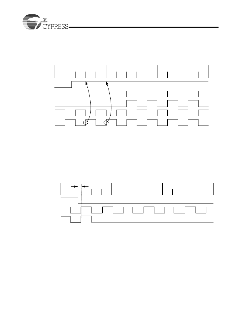
CPU_STOP# Deassertion
The deassertion of the CPU_STOP# signal will cause all
CPUT/C outputs that were stopped to resume normal
operation in a synchronous manner (meaning that no short or
stretched clock pulses will be produces when the clock
resumes). The maximum latency from the deassertion to
active outputs is no more than two CPUC clock cycles.
Three-state Control of CPU Clocks Clarification
During CPU_STOP# and PD# modes, CPU clock outputs may
be set to driven or undriven (tri-state) by setting the corre-
sponding SMBus entry in Bit6 of Byte0 and Bit6 of Byte1.
PCI_STOP# Assertion
The PCI_STOP# signal is an active LOW input used for
synchronous stopping and starting the PCI outputs while the
rest of the clock generator continues to function. The set-up
time for capturing PCI_STOP# going LOW is 10 ns (t
setup
) (see
Figure 2
.) The PCIF clocks will not be affected by this pin if
their control bits in the SMBus register are set to allow them to
be free running.
PCI_STOP# Deassertion
The deassertion of the PCI_STOP# signal will cause all
PCI(0:2, 4:8) and stoppable PCIF clocks to resume running in
a synchronous manner within two PCI clock periods after
PCI_STOP# transitions to a HIGH level.
The PCI STOP function is controlled by two inputs. One is the
device PCI_STOP# pin number 34 and the other is SMBus
Byte 0,Bit 3. These two inputs to the function are logically
AND’ed. If either the external pin or the internal SMBus
register bit is set LOW, the stoppable PCI clocks will be
stopped in a logic LOW state. Reading SMBus Byte 0,Bit 3 will
return a 0 value if either of these control bits are set LOW
(which indicates that the devices stoppable PCI clocks are not
running).
CPU_STP#
CPUT
CPUC
CPUT
CPUC
Figure 6. CPU_STOP# De-assertion Waveform
PCI_STP#
PCIF 33M
PCI 33M
setup
t
Figure 7. PCI_STOP# Assertion Waveform
相關(guān)PDF資料 |
PDF描述 |
|---|---|
| CY28339ZCXT | Intel CK408 Mobile Clock Synthesizer |
| CY28339ZXC | Intel CK408 Mobile Clock Synthesizer |
| CY28339ZC | Intel CK408 Mobile Clock Synthesizer |
| CY28339ZCT | Intel CK408 Mobile Clock Synthesizer |
| CY28339 | Intel CK408 Mobile Clock Synthesizer |
相關(guān)代理商/技術(shù)參數(shù) |
參數(shù)描述 |
|---|---|
| CY28330 | 制造商:CYPRESS 制造商全稱:Cypress Semiconductor 功能描述:Clock Generator for AMD⑩ Hammer |
| CY28330OC | 制造商:Cypress Semiconductor 功能描述: |
| CY28330OCT | 制造商:CYPRESS 制造商全稱:Cypress Semiconductor 功能描述:Clock Generator for AMD⑩ Hammer |
| CY28331 | 制造商:CYPRESS 制造商全稱:Cypress Semiconductor 功能描述:Clock Generator for AMD⑩ Hammer |
| CY28331-2 | 制造商:未知廠家 制造商全稱:未知廠家 功能描述:Clocks and Buffers |
發(fā)布緊急采購(gòu),3分鐘左右您將得到回復(fù)。