- 您現(xiàn)在的位置:買(mǎi)賣(mài)IC網(wǎng) > PDF目錄295174 > BX805499040 (INTEL CORP) 64-BIT, 1600 MHz, MICROPROCESSOR, CPGA611 PDF資料下載
參數(shù)資料
| 型號(hào): | BX805499040 |
| 廠商: | INTEL CORP |
| 元件分類(lèi): | 微控制器/微處理器 |
| 英文描述: | 64-BIT, 1600 MHz, MICROPROCESSOR, CPGA611 |
| 封裝: | PGA-611 |
| 文件頁(yè)數(shù): | 93/108頁(yè) |
| 文件大?。?/td> | 2315K |
| 代理商: | BX805499040 |
第1頁(yè)第2頁(yè)第3頁(yè)第4頁(yè)第5頁(yè)第6頁(yè)第7頁(yè)第8頁(yè)第9頁(yè)第10頁(yè)第11頁(yè)第12頁(yè)第13頁(yè)第14頁(yè)第15頁(yè)第16頁(yè)第17頁(yè)第18頁(yè)第19頁(yè)第20頁(yè)第21頁(yè)第22頁(yè)第23頁(yè)第24頁(yè)第25頁(yè)第26頁(yè)第27頁(yè)第28頁(yè)第29頁(yè)第30頁(yè)第31頁(yè)第32頁(yè)第33頁(yè)第34頁(yè)第35頁(yè)第36頁(yè)第37頁(yè)第38頁(yè)第39頁(yè)第40頁(yè)第41頁(yè)第42頁(yè)第43頁(yè)第44頁(yè)第45頁(yè)第46頁(yè)第47頁(yè)第48頁(yè)第49頁(yè)第50頁(yè)第51頁(yè)第52頁(yè)第53頁(yè)第54頁(yè)第55頁(yè)第56頁(yè)第57頁(yè)第58頁(yè)第59頁(yè)第60頁(yè)第61頁(yè)第62頁(yè)第63頁(yè)第64頁(yè)第65頁(yè)第66頁(yè)第67頁(yè)第68頁(yè)第69頁(yè)第70頁(yè)第71頁(yè)第72頁(yè)第73頁(yè)第74頁(yè)第75頁(yè)第76頁(yè)第77頁(yè)第78頁(yè)第79頁(yè)第80頁(yè)第81頁(yè)第82頁(yè)第83頁(yè)第84頁(yè)第85頁(yè)第86頁(yè)第87頁(yè)第88頁(yè)第89頁(yè)第90頁(yè)第91頁(yè)第92頁(yè)當(dāng)前第93頁(yè)第94頁(yè)第95頁(yè)第96頁(yè)第97頁(yè)第98頁(yè)第99頁(yè)第100頁(yè)第101頁(yè)第102頁(yè)第103頁(yè)第104頁(yè)第105頁(yè)第106頁(yè)第107頁(yè)第108頁(yè)

Dual-Core Intel Itanium Processor 9000 Series Datasheet
85
System Management Feature Specifications
6.3
Scratch EEPROM
Also available on the SMBus interface on the processor is an EEPROM which may be
used for other data at the system vendor’s discretion (Intel will not be using the scratch
EEPROM). The data in this EEPROM, once programmed, can be write-protected by
asserting the active-high SMWP signal. This signal has a weak pull-down (10 kΩ) to
allow the EEPROM to be programmed in systems with no implementation of this signal.
6.4
Processor Information ROM and Scratch EEPROM
Supported SMBus Transactions
The processor information ROM and scratch EEPROM responds to three of the SMBus
packet types: current address read, random address read, and sequential read.
Table 6-5 shows the format of the current address read SMBus packet. The internal
address counter keeps track of the address accessed during the last read or write
operation, incremented by one. Address “roll over” during reads is from the last byte of
the last eight byte page to the first byte of the first page. “Roll over” during writes is
from the last byte of the current eight byte page to the first byte of the same page.
Table 6-6 shows the format of the random read SMBus packet. The write with no data
loads the address desired to be read. Sequential reads may begin with a current
address read or a random address read. After the SMBus host controller receives the
data word, it responds with an acknowledge. This will continue until the SMBus host
controller responds with a negative acknowledge and a stop.
Table 6-7 shows the format of the byte write SMBus packet. The page write operates
the same way as the byte write except that the SMBus host controller does not send a
stop after the first data byte and acknowledge. The Scratch EEPROM internally
increments its address. The SMBus host controller continues to transmit data bytes
until it terminates the sequence with a stop. All data bytes will result in an acknowledge
from the Scratch EEPROM. If more than eight bytes are written, the internal address
will “roll over” and the previous data will be overwritten.
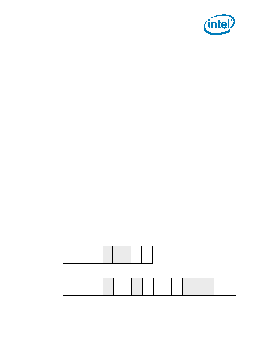
In Table 6-5 through Table 6-7, ‘S’ represents the SMBus start bit, ‘P’ represents a stop
bit, ‘R’ represents a read, ‘W’ represents a write bit, ‘A’ represents an acknowledge, and
‘///’ represents a negative acknowledge. The shaded bits are transmitted by the
processor information ROM or Scratch EEPROM and the bits that are not shaded are
transmitted by the SMBus host controller. In the tables the data addresses indicate
eight bits. The SMBus host controller should transmit eight bits, but as there are only
128 addresses, the most significant bit is a don’t care.
Table 6-5.
Current Address Read SMBus Packet
S
Device
Address
R
A
Data
///
P
17 bits
1
8 bits
1
Table 6-6.
Random Address Read SMBus Packet
S
Device
Address
W
A
Data
Address
AS
Device
Address
R
A
Data
///
P
17 bits
1
18 bits
11
7 bits
1
8 bits
1
相關(guān)PDF資料 |
PDF描述 |
|---|---|
| BXA10-12D15-S | 2-OUTPUT DC-DC REG PWR SUPPLY MODULE |
| BXA200-48S12 | 1-OUTPUT 200 W DC-DC REG PWR SUPPLY MODULE |
| BXA40-48S15 | 1-OUTPUT 40 W DC-DC REG PWR SUPPLY MODULE |
| BXB100-48S15FLTJ | 1-OUTPUT 100 W DC-DC REG PWR SUPPLY MODULE |
| BXB75-48S12FHTJ | 1-OUTPUT 75 W DC-DC REG PWR SUPPLY MODULE |
相關(guān)代理商/技術(shù)參數(shù) |
參數(shù)描述 |
|---|---|
| BX805499050 | 制造商:Intel 功能描述:ITANIUM PROCESSOR 1.6 GHZ - Boxed Product (Development Kits) |
| BX80551KG2800HUS L8MA | 制造商:Intel 功能描述:BOXED INTEL XEON PROCESSOR 2.80 GHZ, 4M CACHE, 800 MHZ FSB, PASSIVE, FC-MPGA |
| BX80551PE2666FNS L8ZH | 制造商:Intel 功能描述:MPU PENTIUM D 90NM 2.66GHZ 775PIN FCLGA4 - Boxed Product (Development Kits) |
| BX80552352 S L96P | 制造商:Intel 功能描述:MPU Celeron 制造商:Intel 功能描述:MPU Celeron? D Processor 352 65nm 3.2GHz 775-Pin FCLGA4 |
| BX80552360 S L9KK | 制造商:Intel 功能描述:MPU CELERON 65NM 3.46GHZ 775PIN FCLGA4 - Boxed Product (Development Kits) |
發(fā)布緊急采購(gòu),3分鐘左右您將得到回復(fù)。