- 您現(xiàn)在的位置:買賣IC網(wǎng) > PDF目錄366551 > AM79C976 (Advanced Micro Devices, Inc.) PCnet-PRO⑩ 10/100 Mbps PCI Ethernet Controller PDF資料下載
參數(shù)資料
| 型號: | AM79C976 |
| 廠商: | Advanced Micro Devices, Inc. |
| 英文描述: | PCnet-PRO⑩ 10/100 Mbps PCI Ethernet Controller |
| 中文描述: | PCnet -專業(yè)⑩個10/100Mbps PCI以太網(wǎng)控制器 |
| 文件頁數(shù): | 59/309頁 |
| 文件大小: | 2070K |
| 代理商: | AM79C976 |
第1頁第2頁第3頁第4頁第5頁第6頁第7頁第8頁第9頁第10頁第11頁第12頁第13頁第14頁第15頁第16頁第17頁第18頁第19頁第20頁第21頁第22頁第23頁第24頁第25頁第26頁第27頁第28頁第29頁第30頁第31頁第32頁第33頁第34頁第35頁第36頁第37頁第38頁第39頁第40頁第41頁第42頁第43頁第44頁第45頁第46頁第47頁第48頁第49頁第50頁第51頁第52頁第53頁第54頁第55頁第56頁第57頁第58頁當前第59頁第60頁第61頁第62頁第63頁第64頁第65頁第66頁第67頁第68頁第69頁第70頁第71頁第72頁第73頁第74頁第75頁第76頁第77頁第78頁第79頁第80頁第81頁第82頁第83頁第84頁第85頁第86頁第87頁第88頁第89頁第90頁第91頁第92頁第93頁第94頁第95頁第96頁第97頁第98頁第99頁第100頁第101頁第102頁第103頁第104頁第105頁第106頁第107頁第108頁第109頁第110頁第111頁第112頁第113頁第114頁第115頁第116頁第117頁第118頁第119頁第120頁第121頁第122頁第123頁第124頁第125頁第126頁第127頁第128頁第129頁第130頁第131頁第132頁第133頁第134頁第135頁第136頁第137頁第138頁第139頁第140頁第141頁第142頁第143頁第144頁第145頁第146頁第147頁第148頁第149頁第150頁第151頁第152頁第153頁第154頁第155頁第156頁第157頁第158頁第159頁第160頁第161頁第162頁第163頁第164頁第165頁第166頁第167頁第168頁第169頁第170頁第171頁第172頁第173頁第174頁第175頁第176頁第177頁第178頁第179頁第180頁第181頁第182頁第183頁第184頁第185頁第186頁第187頁第188頁第189頁第190頁第191頁第192頁第193頁第194頁第195頁第196頁第197頁第198頁第199頁第200頁第201頁第202頁第203頁第204頁第205頁第206頁第207頁第208頁第209頁第210頁第211頁第212頁第213頁第214頁第215頁第216頁第217頁第218頁第219頁第220頁第221頁第222頁第223頁第224頁第225頁第226頁第227頁第228頁第229頁第230頁第231頁第232頁第233頁第234頁第235頁第236頁第237頁第238頁第239頁第240頁第241頁第242頁第243頁第244頁第245頁第246頁第247頁第248頁第249頁第250頁第251頁第252頁第253頁第254頁第255頁第256頁第257頁第258頁第259頁第260頁第261頁第262頁第263頁第264頁第265頁第266頁第267頁第268頁第269頁第270頁第271頁第272頁第273頁第274頁第275頁第276頁第277頁第278頁第279頁第280頁第281頁第282頁第283頁第284頁第285頁第286頁第287頁第288頁第289頁第290頁第291頁第292頁第293頁第294頁第295頁第296頁第297頁第298頁第299頁第300頁第301頁第302頁第303頁第304頁第305頁第306頁第307頁第308頁第309頁
8/01/00
Am79C976
59
P R E L I M I N A R Y
/%
Note that the Am79C976 controller will always perform
a DWord transfer as long as it owns the buffer space,
even when there are less than four bytes to write. For
example, if there is only one byte left for the current re-
ceive frame, the Am79C976 controller will write a full
DWord, containing the last byte of the receive frame in
the least significant byte position (BSWP is cleared to
0, CSR3, bit 2). The content of the other three bytes is
undefined. The message byte count in the receive
descriptor always reflects the exact length of the re-
ceived frame.
In the normal DMA mode (when the Burst Alignment bit
= 0 and the Burst Limit register contents = 0) the
Am79C976 controller will continue transferring FIFO
data until the transmit FIFO is filled to its high threshold
(for read transfers) or the receive FIFO is emptied to its
low threshold (for write transfers), or until the
Am79C976 controller is preempted and the PCI La-
tency Timer is expired. The host should use the values
in the PCI MIN_GNT and MAX_LAT registers to deter-
mine the value for the PCI Latency Timer.
In the burst alignment mode (when the Burst Alignment
bit = 1) if a burst transfer starts in the middle of a cache
line, the transfer will stop at the first cache line
boundary.
If the contents of the Burst Limit register are not zero, a
burst transfer will end when the transfer has crossed
the number of cache line boundaries equal to the con-
tents of this register.
The exact number of total transfer cycles in the bus
mastership period is dependent on all of the following
variables: the settings of the FIFO watermarks, the
conditions of the FIFOs, the latency of the system bus
to the Am79C976 controller
’
s bus request, and the
speed of bus operation. The TRDY response time of
the memory device will also affect the number of trans-
fers, since the speed of the accesses will affect the
state of the FIFO. The general rule is that the longer the
Bus Grant latency, the slower the bus transfer opera-
tions; the slower the clock speed, the higher the trans-
mit watermark; or the lower the receive watermark, the
longer the total burst length will be.
When a FIFO DMA burst operation is preempted, the
Am79C976 controller will not relinquish bus ownership
until the PCI Latency Timer expires.
Descriptor Management Unit
The Descriptor Management Unit (DMU) implements
the automatic initialization procedure and manages the
descriptors and buffers.
6
The Am79C976 controller is initialized by a combina-
tion of EEPROM register writes, direct register writes
from the PCI bus and, for compatibility with older PCnet
family products, DMA reads from an initialization block
in memory. The registers that must be programmed de-
pend on the features that are required in a particular
application. See
USER ACCESSIBLE REGISTERS on
page 111
for more details.
The format of the legacy initialization block depends on
the programming of the SWSTYLE register, as de-
scribed in the
Initialization Block
section.
The initialization block is read when the INIT bit in
CSR0 is set. The INIT bit should be set before or con-
current with the STRT bit to ensure correct operation.
Once the initialization block has been completely read
in and internal registers have been updated, IDON will
be set in CSR0, generating an interrupt (if IENA is set).
The Am79C976 controller obtains the start address of
the initialization block from the contents of CSR1 (least
significant 16 bits of address) and CSR2 (most signifi-
cant 16 bits of address). The host must write CSR1 and
CSR2 before setting the INIT bit. The initialization block
contains the user defined conditions for Am79C976 op-
eration, together with the base addresses and length
information of the transmit and receive descriptor rings.
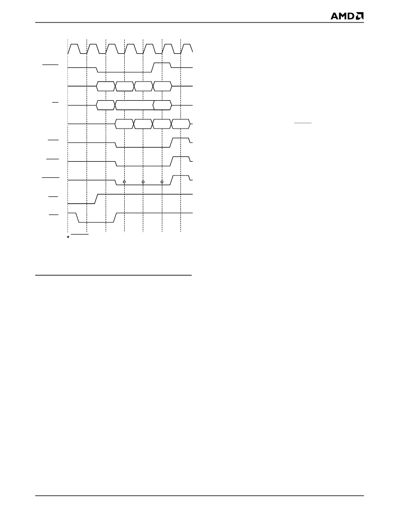
FRAME
CLK
AD
IRDY
TRDY
C/BE
DEVSEL
REQ
GNT
1
2
3
4
5
6
7
0000
0111
PAR
PAR
PAR
PAR
DEVSEL is sampled
1110
PAR
DATA
DATA
DATA
ADD
相關(guān)PDF資料 |
PDF描述 |
|---|---|
| AM79C976KIW | PCnet-PRO⑩ 10/100 Mbps PCI Ethernet Controller |
| AM79C976KCW | PCnet-PRO⑩ 10/100 Mbps PCI Ethernet Controller |
| AM79C978AKCW | Single-Chip 1/10 Mbps PCI Home Networking Controller |
| AM79C978AVCW | Single-Chip 1/10 Mbps PCI Home Networking Controller |
| AM79C978 | Single-Chip 1/10 Mbps PCI Home Networking Controller |
相關(guān)代理商/技術(shù)參數(shù) |
參數(shù)描述 |
|---|---|
| AM79C976KC | 制造商:Rochester Electronics LLC 功能描述:METRIC PLASTIC QUAD-RING - Bulk |
| AM79C976KCW | 制造商:AMD 制造商全稱:Advanced Micro Devices 功能描述:PCnet-PRO⑩ 10/100 Mbps PCI Ethernet Controller |
| AM79C976KD | 制造商:Advanced Micro Devices 功能描述:ETHERNET:MEDIA ACCESS CONTROLLER (MAC) |
| AM79C976KF | 制造商:Advanced Micro Devices 功能描述:Ethernet CTLR Single Chip 10Mbps/100Mbps 3.3V 208-Pin PQFP 制造商:AMD (Advanced Micro Devices) 功能描述:Ethernet CTLR Single Chip 10Mbps/100Mbps 3.3V 208-Pin PQFP |
| AM79C976KI | 制造商:Advanced Micro Devices 功能描述:Ethernet CTLR Single Chip 10Mbps/100Mbps 3.3V 208-Pin PQFP 制造商:AMD (Advanced Micro Devices) 功能描述:Ethernet CTLR Single Chip 10Mbps/100Mbps 3.3V 208-Pin PQFP |
發(fā)布緊急采購,3分鐘左右您將得到回復(fù)。