- 您現(xiàn)在的位置:買賣IC網(wǎng) > PDF目錄298821 > AM29LV640MH101EF (SPANSION LLC) 4M X 16 FLASH 3V PROM, 100 ns, PDSO56 PDF資料下載
參數(shù)資料
| 型號(hào): | AM29LV640MH101EF |
| 廠商: | SPANSION LLC |
| 元件分類: | PROM |
| 英文描述: | 4M X 16 FLASH 3V PROM, 100 ns, PDSO56 |
| 封裝: | MO-142B, TSOP-56 |
| 文件頁數(shù): | 49/59頁 |
| 文件大?。?/td> | 1590K |
| 代理商: | AM29LV640MH101EF |
第1頁第2頁第3頁第4頁第5頁第6頁第7頁第8頁第9頁第10頁第11頁第12頁第13頁第14頁第15頁第16頁第17頁第18頁第19頁第20頁第21頁第22頁第23頁第24頁第25頁第26頁第27頁第28頁第29頁第30頁第31頁第32頁第33頁第34頁第35頁第36頁第37頁第38頁第39頁第40頁第41頁第42頁第43頁第44頁第45頁第46頁第47頁第48頁當(dāng)前第49頁第50頁第51頁第52頁第53頁第54頁第55頁第56頁第57頁第58頁第59頁
February 16, 2003
Am29LV640MH/L
53
ADV ANCE
I N FO RMAT I O N
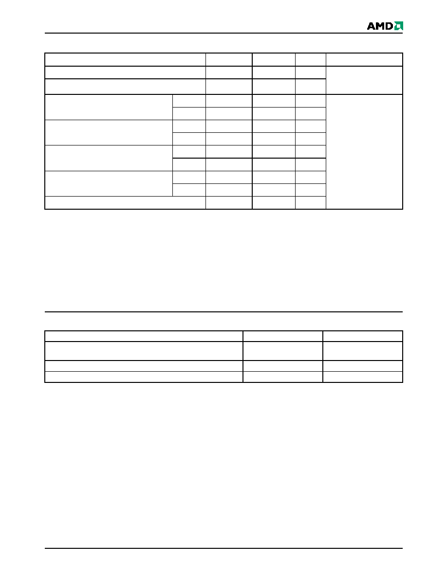
ERASE AND PROGRAMMING PERFORMANCE
Notes:
1. Typical program and erase times assume the following conditions: 25
°C, 3.0 V V
CC, 100,000 cycles. Additionally,
programming typicals assume checkerboard pattern.
2. Under worst case conditions of 90
°C, V
CC = 3.0 V, 100,000 cycles.
3. Effective write buffer specification is based upon a 16-word/32-byte write buffer operation.
4. Word/Byte programming specification is based upon a single word/byte programming operation not utilizing the write buffer.
5. The typical chip programming time is considerably less than the maximum chip programming time listed, since most words
program faster than the maximum program times listed.
6. In the pre-programming step of the Embedded Erase algorithm, all bits are programmed to 00h before erasure.
7. System-level overhead is the time required to execute the two- or four-bus-cycle sequence for the program command. See Tables
12 and 11 for further information on command definitions.
8. The device has a minimum erase and program cycle endurance of 100,000 cycles.
LATCHUP CHARACTERISTICS
Note: Includes all pins except V
CC. Test conditions: VCC = 3.0 V, one pin at a time.
Parameter
Typ (Note 1)
Max (Note 2)
Unit
Comments
Sector Erase Time
0.5
15
sec
Excludes 00h
programming
prior to erasure (Note 6)
Chip Erase Time
64
TBD
sec
Effective Write Buffer Program Time (Note 3)
Per Byte
11
TBD
s
Excludes system level
overhead (Note 7)
Per Word
22
TBD
s
Accelerated Effective Write Buffer Program
Time (Note 3)
Per Byte
8.8
TBD
s
Per Word
17.6
TBD
s
Single Byte/Word Program Time (Note 4)
Byte
100
TBD
s
Word
100
TBD
s
Accelerated Single Byte/Word Program Time
(Note 4)
Byte
90
TBD
s
Word
90
TBD
s
Chip Program Time (Note 5)
92
TBD
sec
Description
Min
Max
Input voltage with respect to V
SS on all pins except I/O pins
(including A9, OE#, and RESET#)
–1.0 V
12.5 V
Input voltage with respect to V
SS on all I/O pins
–1.0 V
V
CC + 1.0 V
V
CC Current
–100 mA
+100 mA
相關(guān)PDF資料 |
PDF描述 |
|---|---|
| AM2D-11G | ACTIVE DELAY LINE, TRUE OUTPUT, PDSO8 |
| AI4D-4J | ACTIVE DELAY LINE, TRUE OUTPUT, PDSO14 |
| AM3D-11J | ACTIVE DELAY LINE, TRUE OUTPUT, PDSO8 |
| AM3D-25J | ACTIVE DELAY LINE, TRUE OUTPUT, PDSO8 |
| AM3D-35J | ACTIVE DELAY LINE, TRUE OUTPUT, PDSO8 |
相關(guān)代理商/技術(shù)參數(shù) |
參數(shù)描述 |
|---|---|
| AM29LV640MH112REI | 制造商:Advanced Micro Devices 功能描述:4M X 16 FLASH 3V PROM, 110 ns, PDSO56 |
| AM29LV640MU101RPCI | 制造商:Advanced Micro Devices 功能描述: |
| AM29LV640MU90NI | 制造商:Advanced Micro Devices 功能描述: |
| AM29LV640MU90RPC1 | 制造商:Advanced Micro Devices 功能描述: |
| AM29LV640MU90RPCI | 制造商:Advanced Micro Devices 功能描述: |
發(fā)布緊急采購,3分鐘左右您將得到回復(fù)。