- 您現(xiàn)在的位置:買(mǎi)賣(mài)IC網(wǎng) > PDF目錄373859 > AD1815 (Analog Devices, Inc.) SoundComm Controller(SoundComm 控制器) PDF資料下載
參數(shù)資料
| 型號(hào): | AD1815 |
| 廠商: | Analog Devices, Inc. |
| 英文描述: | SoundComm Controller(SoundComm 控制器) |
| 中文描述: | SoundComm控制器(SoundComm控制器) |
| 文件頁(yè)數(shù): | 38/44頁(yè) |
| 文件大小: | 426K |
| 代理商: | AD1815 |
第1頁(yè)第2頁(yè)第3頁(yè)第4頁(yè)第5頁(yè)第6頁(yè)第7頁(yè)第8頁(yè)第9頁(yè)第10頁(yè)第11頁(yè)第12頁(yè)第13頁(yè)第14頁(yè)第15頁(yè)第16頁(yè)第17頁(yè)第18頁(yè)第19頁(yè)第20頁(yè)第21頁(yè)第22頁(yè)第23頁(yè)第24頁(yè)第25頁(yè)第26頁(yè)第27頁(yè)第28頁(yè)第29頁(yè)第30頁(yè)第31頁(yè)第32頁(yè)第33頁(yè)第34頁(yè)第35頁(yè)第36頁(yè)第37頁(yè)當(dāng)前第38頁(yè)第39頁(yè)第40頁(yè)第41頁(yè)第42頁(yè)第43頁(yè)第44頁(yè)
AD1815
–38–
REV. 0
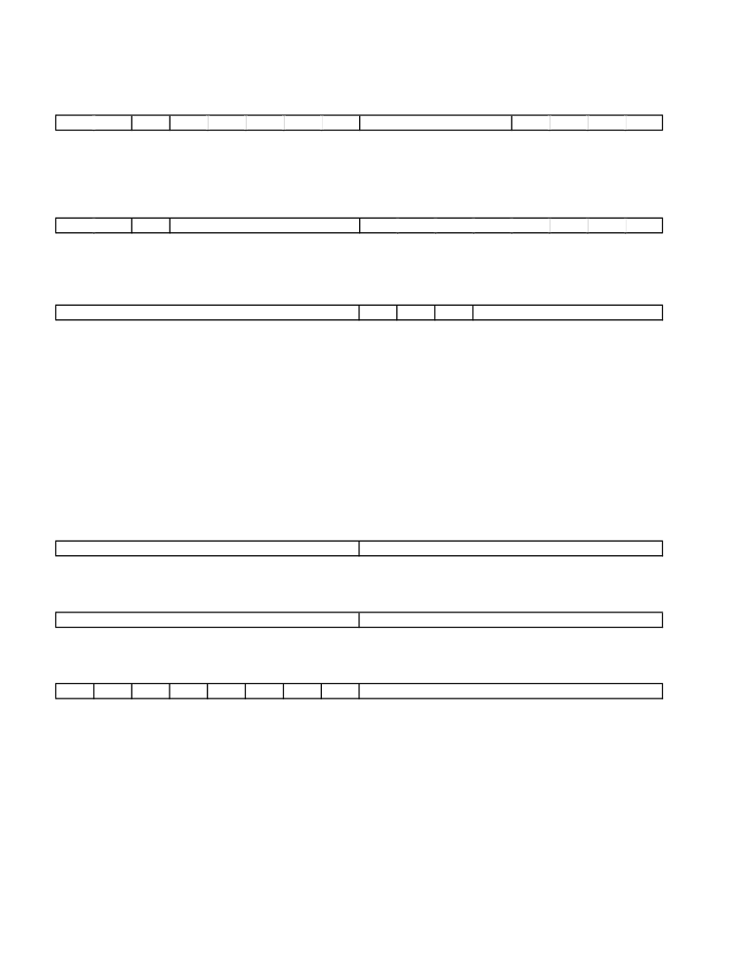
[39] MODEM DAC and ADC Attenuation
7
6
5
M D M
RES
DEFAULT = [0x8000]
2
MAG [3:0]
4
3
2
1
0
7
6
5
4
3
1
0
MDA [4:0]
RES
MAG [3:0]
MDA [4:0]
MDM
Modem ADC Gain. T he LSB represents +1.5 dB and the range is 0 dB to +22.5 dB.
Modem DAC Attenuation. T he LSB represents 1 dB and the range is 0 dB to –31 dB.
Modem DAC Mute.
[40] MODEM MIX Attenuation
7
6
MMM
RES
DEFAULT = [0x80XX]
2
5
4
3
2
1
0
7
6
5
4
3
1
0
MDA [4:0]
RES
MDA [4:0]
MMM
MODEM-IN Attenuation. T he LSB represents –1.5 dB, 00000 = +12 dB and the range is +12 dB to –34.5 dB
MODEM Mix Mute.
[41] HARDWARE VOLUME BUTTON MODIFIER and STATUS
7
6
5
4
3
RES
DEFAULT = [0xXX1B]
2
BM [4:0]
2
1
0
7
6
5
4
3
1
0
VMU
VUP
VDN
BM [4:0]
VDM
VUP
VMU
T his register contains a MAST ER VOLUME attenuation offset that can be incremented or decremented via the Hardware
Volume Pins. T his Register is summed with the MAST ER VOLUME attenuation to produce the actual MAST ER VOLUME
DAC attenuation. A momentary press of greater than 50 ms on the VOLUME-UP pin will cause a decrement (decrease in
Attenuation) in this register. Holding the pin for greater than 200 ms will cause an auto-decrement every 200 ms. T his is also
true for a momentary press of the VOLUME-DOWN pin. A momentary press of both the VOLUME-UP and VOLUME-DOWN
causes a mute and no increment or decrement to occur.
When Muted, an un-mute is possible by either a momentary press of both the VOLUME-UP and VOLUME-DOWN pins
together, a momentary press of VOLUME-UP (this also causes a volume increase), a momentary press of VOLUME-DOWN
(this also causes a volume decrease) or a write of “0” to the VI bit in SS[BASE+1].
Button Modifier
Volume Down
Volume Up
Volume Mute
[42] DSP MAILBOX 0
7
6
DEFAULT = [0x0000]
2
5
4
3
2
1
0
7
6
5
4
3
1
0
MB0R [15:8]
MB0R [7:0]
MB0R [15:0]
T his register is used to send data and control information to and from the DSP.
[43] DSP MAILBOX 1
7
6
DEFAULT = [0x0000]
2
5
4
3
2
1
0
7
6
5
4
3
1
0
MB1R [15:8]
MB1R [7:0]
MB1R [15:0]
T his register is used to send data and control information to and from the DSP.
[44] POWERDOWN and TIMER CONTROL
7
6
5
C PD
RES
PIW
DEFAULT = [0x0000]
2
4
3
2
1
0
7
6
5
4
3
1
0
PIR
PAA
PDA
PD P
PT B
RES
T he AD1815 supports a time-out mechanism used in conjunction with the T IMER BASE COUNT /T IMER CURRENT
COUNT registers to generate a powerdown interrupt. T his interrupt allows software to powerdown the entire chip by setting the
CPD bit. T his powerdown control feature lets users program a time interval from 1 ms to approximately 1.8 hours in
1 ms increments. Five powerdown count reload enable bits are used to reload the T IMER CURRENT COUNT from
the T IMER BASE COUNT when activity is seen on that particular channel.
Programming Example: Generate Interrupt if No ISA Reads or Writes occur within 15 Minutes.
1) Write [SSBASE+0] with 0x0C ; Write Indirect address for T IMER BASE COUNT “register 12”
2) Write [SSBASE+2] with 0x28 ; Write T IMER BASE COUNT with (15min * 60sec/min * 10) = 0x2328 mili-Seconds
3) Write [SSBASE+3] with 0x23 ; Write High byte of T IMER BASE COUNT
4) Write [SSBASE+0] with 0x2C ; Write Indirect address for POWERDOWN and T IMER CONT ROL register
5) Write [SSBASE+2] with 0x00 ; Write Low byte of POWERDOWN and T IMER CONT ROL register
6) Write [SSBASE+3] with 0x30 ; Set Enable bits for PIW & PIR
7) Write [SSBASE+0] with 0x01 ; Write Indirect address for INT ERRUPT CONFIG register
8) Write [SSBASE+2] with 0x82 ; Set the T E (T imer Enable) bit
9) Write [SSBASE+3] with 0x20 ; Set the T IE (T imer Interrupt Enable) bit
相關(guān)PDF資料 |
PDF描述 |
|---|---|
| AD1816AJS | SoundPort Controller |
| AD1816AJST | SoundPort Controller |
| AD1816A | SoundPort Controller(數(shù)字音頻的聲音端口控制器) |
| AD1818 | PCI SoundComm DC97 Digital Controller(PCI SoundComm DC97型數(shù)字控制器) |
| AD1819A | AC97 SoundPort Codec(AC97型聲音端口信號(hào)編解碼器) |
相關(guān)代理商/技術(shù)參數(shù) |
參數(shù)描述 |
|---|---|
| AD1815JS | 制造商:Rochester Electronics LLC 功能描述:- Bulk 制造商:Analog Devices 功能描述: |
| AD1816A | 制造商:AD 制造商全稱(chēng):Analog Devices 功能描述:SoundPort Controller |
| AD1816AJS | 制造商:AD 制造商全稱(chēng):Analog Devices 功能描述:SoundPort Controller |
| ad1816ajs-eeprom | 制造商:Rochester Electronics LLC 功能描述:AD1816A SOUND PORT CONTRO - Bulk 制造商:Analog Devices 功能描述: |
| AD1816AJST | 制造商:AD 制造商全稱(chēng):Analog Devices 功能描述:SoundPort Controller |
發(fā)布緊急采購(gòu),3分鐘左右您將得到回復(fù)。