- 您現(xiàn)在的位置:買賣IC網(wǎng) > PDF目錄298480 > 70V3319S166BFG (INTEGRATED DEVICE TECHNOLOGY INC) 256K X 18 DUAL-PORT SRAM, 3.6 ns, CBGA208 PDF資料下載
參數(shù)資料
| 型號(hào): | 70V3319S166BFG |
| 廠商: | INTEGRATED DEVICE TECHNOLOGY INC |
| 元件分類: | SRAM |
| 英文描述: | 256K X 18 DUAL-PORT SRAM, 3.6 ns, CBGA208 |
| 封裝: | 15 X 15 MM X 1.4 MM, 0.80 MM PITCH, GREEN, FPBGA-208 |
| 文件頁數(shù): | 20/23頁 |
| 文件大小: | 222K |
| 代理商: | 70V3319S166BFG |

6.42
IDT70V3319/99S
High-Speed 3.3V 256/128K x 18 Dual-Port Synchronous Static RAM
Industrial and Commercial Temperature Ranges
6
NOTES:
1. "H" = VIH, "L" = VIL, "X" = Don't Care.
2.
ADS, CNTEN, REPEAT = X.
3.
OE is an asynchronous input signal.
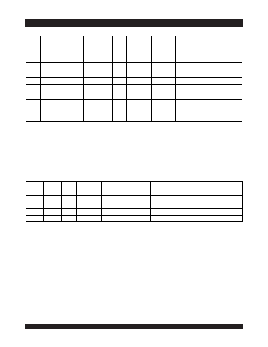
Truth Table I—Read/Write and Enable Control(1,2,3)
OE
CLK
CE0
CE1
UB
LB
R/
W
Upper Byte
I/O9-17
Lower Byte
I/O0-8
MODE
X
↑
H
XXXX
High-Z
Deselected–Power Down
X
↑
X
L
X
High-Z
Deselected–Power Down
X
↑
L
H
X
High-Z
Both Bytes Deselected
X
↑
LH
H
L
High-Z
DIN
Write to Lower Byte Only
X
↑
LH
L
DIN
High-Z
Write to Upper Byte Only
X
↑
L
H
LLL
DIN
Write to Both Bytes
L
↑
LH
H
L
H
High-Z
DOUT
Read Lower Byte Only
L
↑
LH
H
DOUT
High-Z
Read Upper Byte Only
L
↑
LH
L
H
DOUT
Read Both Bytes
H
↑
L
H
L
X
High-Z
Outputs Disabled
5623 tbl 02
Truth Table II—Address Counter Control(1,2)
NOTES:
1. "H" = VIH, "L" = VIL, "X" = Don't Care.
2. Read and write operations are controlled by the appropriate setting of R/
W, CE0, CE1, UB, LB and OE.
3. Outputs configured in flow-through output mode: if outputs are in pipelined mode the date out will be delayed by one cycle.
4.
ADS and REPEAT are independent of all other memory control signals including CE0, CE1 and UB, LB.
5. The address counter advances if
CNTEN = VIL on the rising edge of CLK, regardless of all other memory control signals including CE0, CE1, UB, LB.
6. When
REPEAT is asserted, the counter will reset to the last valid address loaded via ADS. This value is not set at power-up: a known location should be loaded
via
ADS during initialization if desired. Any subsequent ADS access during operations will update the REPEAT address location.
External
Address
Previous
Internal
Address
Internal
Address
Used
CLK
ADS
CNTEN
REPEAT(6)
I/O(3)
MODE
XX
An
↑
XX
L(4)
DI/O(0)
Counter Reset to last valid
ADS load
An
X
An
↑
L(4)
XH
DI/O (n)
External Address Used
An
Ap
↑
HH
H
DI/O(p)
External Address Blocked—Counter disabled (Ap reused)
XAp
Ap + 1
↑
H
L(5)
HDI/O(p+1)
Counter Enabled—Internal Address generation
5623 tbl 03
相關(guān)PDF資料 |
PDF描述 |
|---|---|
| 70V3319S133BCGI | 256K X 18 DUAL-PORT SRAM, 4.2 ns, CBGA256 |
| 70V9389L9PRFI8 | 64K X 18 DUAL-PORT SRAM, 20 ns, PQFP128 |
| IDT70V9289L9PRF8 | 64K X 16 DUAL-PORT SRAM, 20 ns, PQFP128 |
| 710026-3 | 25 mm2, COPPER ALLOY, TIN FINISH, WIRE TERMINAL |
| 710027-5 | 35 mm2, COPPER ALLOY, TIN FINISH, WIRE TERMINAL |
相關(guān)代理商/技術(shù)參數(shù) |
參數(shù)描述 |
|---|---|
| 70V3319S166BFG8 | 制造商:Integrated Device Technology Inc 功能描述:SRAM Chip Sync Dual 3.3V 4.5M-Bit 256K x 18 12ns/3.6ns 208-Pin CABGA T/R 制造商:Integrated Device Technology Inc 功能描述:SRAM SYNC DUAL 3.3V 4MBIT 256KX18 12NS/3.6NS 208FPBGA - Tape and Reel 制造商:Integrated Device Technology Inc 功能描述:256Kx18 STD-PWR 3.3V SYNC DUAL-PORT RAM |
| 70V3319S166PRF | 功能描述:靜態(tài)隨機(jī)存取存儲(chǔ)器 256Kx18 STD-PWR 3.3V SYNC DUAL-PORT RAM RoHS:否 制造商:Cypress Semiconductor 存儲(chǔ)容量:16 Mbit 組織:1 M x 16 訪問時(shí)間:55 ns 電源電壓-最大:3.6 V 電源電壓-最小:2.2 V 最大工作電流:22 uA 最大工作溫度:+ 85 C 最小工作溫度:- 40 C 安裝風(fēng)格:SMD/SMT 封裝 / 箱體:TSOP-48 封裝:Tray |
| 70V3319S166PRF8 | 制造商:Integrated Device Technology Inc 功能描述:SRAM Chip Sync Dual 3.3V 4.5M-Bit 256K x 18 12ns/3.6ns 128-Pin TQFP T/R 制造商:Integrated Device Technology Inc 功能描述:SRAM SYNC DUAL 3.3V 4MBIT 256KX18 12NS/3.6NS 128TQFP - Tape and Reel 制造商:Integrated Device Technology Inc 功能描述:256Kx18 STD-PWR 3.3V SYNC DUAL-PORT RAM |
| 70V3319S166PRFG | 功能描述:靜態(tài)隨機(jī)存取存儲(chǔ)器 256Kx18 STD-PWR 3.3V SYNC DUAL-PORT RAM RoHS:否 制造商:Cypress Semiconductor 存儲(chǔ)容量:16 Mbit 組織:1 M x 16 訪問時(shí)間:55 ns 電源電壓-最大:3.6 V 電源電壓-最小:2.2 V 最大工作電流:22 uA 最大工作溫度:+ 85 C 最小工作溫度:- 40 C 安裝風(fēng)格:SMD/SMT 封裝 / 箱體:TSOP-48 封裝:Tray |
| 70V3319S166PRFG8 | 制造商:Integrated Device Technology Inc 功能描述:SRAM Chip Sync Dual 3.3V 4.5M-Bit 256K x 18 12ns/3.6ns 128-Pin TQFP T/R 制造商:Integrated Device Technology Inc 功能描述:SRAM SYNC DUAL 3.3V 4MBIT 256KX18 12NS/3.6NS 128TQFP - Tape and Reel 制造商:Integrated Device Technology Inc 功能描述:256Kx18 STD-PWR 3.3V SYNC DUAL-PORT RAM |
發(fā)布緊急采購,3分鐘左右您將得到回復(fù)。