- 您現(xiàn)在的位置:買賣IC網(wǎng) > PDF目錄373786 > ZL50212 (Zarlink Semiconductor Inc.) 288 Channel Voice Echo Canceller PDF資料下載
參數(shù)資料
| 型號(hào): | ZL50212 |
| 廠商: | Zarlink Semiconductor Inc. |
| 英文描述: | 288 Channel Voice Echo Canceller |
| 中文描述: | 288頻道語音回聲消除器 |
| 文件頁數(shù): | 28/43頁 |
| 文件大小: | 2166K |
| 代理商: | ZL50212 |
第1頁第2頁第3頁第4頁第5頁第6頁第7頁第8頁第9頁第10頁第11頁第12頁第13頁第14頁第15頁第16頁第17頁第18頁第19頁第20頁第21頁第22頁第23頁第24頁第25頁第26頁第27頁當(dāng)前第28頁第29頁第30頁第31頁第32頁第33頁第34頁第35頁第36頁第37頁第38頁第39頁第40頁第41頁第42頁第43頁
ZL50212
Data Sheet
28
Zarlink Semiconductor Inc.
9.0
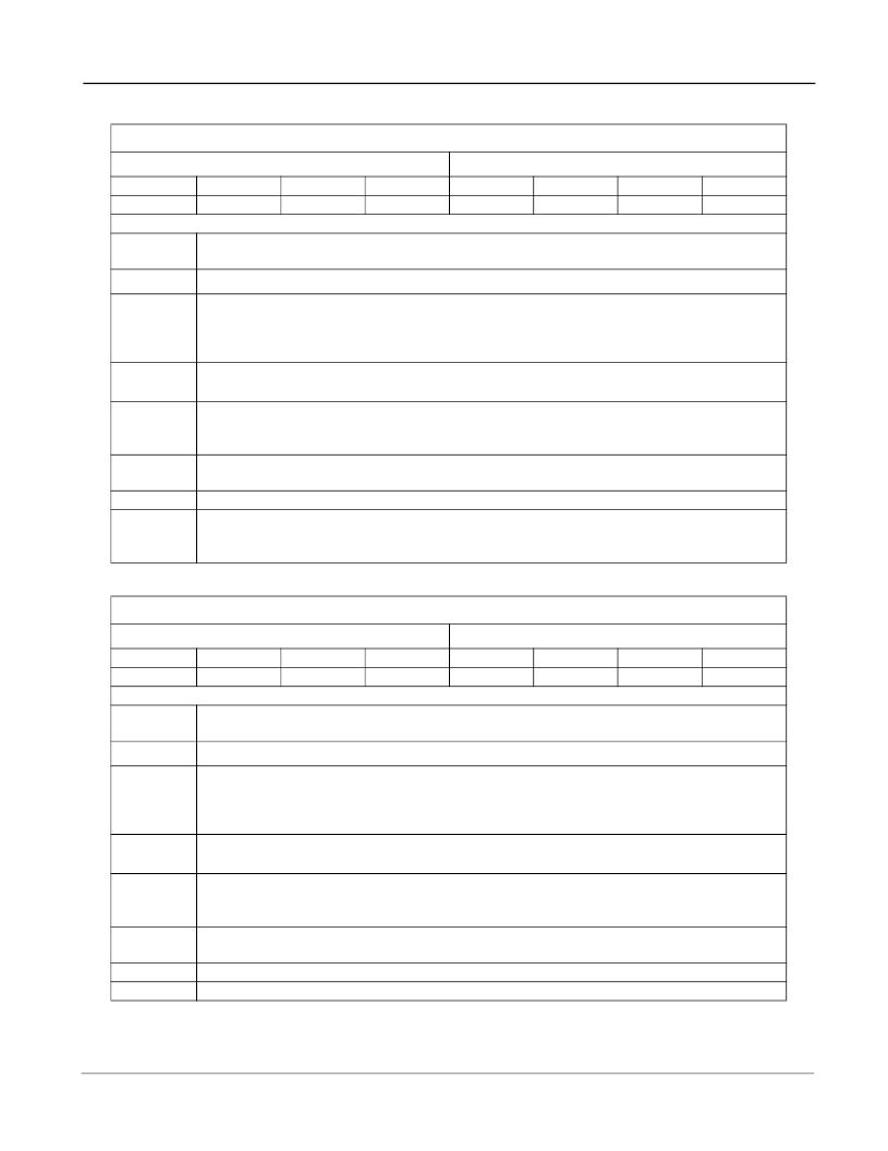
EVP Registers Description
Note: In order to correctly write to Control Register 1 and 2 of ECB, it is necessary to write the data twice to the register, one
immediately after another. The two writes must be separated by at least 350ns and no more than 20us.
Echo Canceller A (ECA): Control Register 1
Power-up 00
hex
Bit 6
INJDis
R/W Address: 00
hex
+ Base Address
Bit 3
Bit 2
Bypass
AdpDis
Bit 7
Reset
Bit 5
BBM
Functional Description of Register Bits
When high, the power-up initialization is executed. This presets all register bits including
this bit and clears the Adaptive Filter coefficients.
When high, the noise injection process is disabled. When low noise injection is enabled.
Bit 4
PAD
Bit 1
0
Bit 0
ExtDI
Reset
INJDis
BBM
When high, the Back to Back configuration is enabled. When low, the Normal
configuration is enabled. Note: Do not enable Extended-Delay and BBM configurations at
the same time. Always set
both
BBM bits of the two echo cancellers (Control Register 1)
of the same group to the same logic value to avoid conflict.
PAD
When high, 12dB of attenuation is inserted into the Rin to Rout path. When low, the Gains
register controls the signal levels.
When high, Sin data is by-passed to Sout and Rin data is by-passed to Rout. The
Adaptive Filter coefficients are set to zero and the filter adaptation is stopped. When low,
output data on both Sout and Rout is a function of the echo canceller algorithm.
When high, echo canceller adaptation is disabled. The Voice Processor cancels echo.
When low, the echo canceller dynamically adapts to the echo path characteristics.
Bits marked as “1” or “0” are reserved bits and should be written as indicated.
When high, Echo Cancellers A and B of the same group are internally cascaded into one
128ms echo canceller. When low, Echo Cancellers A and B of the same group operate
independently.
Bypass
AdpDis
0
ExtDl
Echo Canceller B (ECB): Control Register 1
Power-up 02
hex
Bit 6
INJDis
R/W Address: 20
hex
+ Base Address
Bit 3
Bit 2
Bypass
AdpDis
Bit 7
Reset
Bit 5
BBM
Functional Description of Register Bits
When high, the power-up initialization is executed which presets all register bits including
this bit and clears the Adaptive Filter coefficients.
When high, the noise injection process is disabled. When low, noise injection is enabled.
Bit 4
PAD
Bit 1
1
Bit 0
0
Reset
INJDis
BBM
When high, the Back to Back configuration is enabled. When low, the Normal
configuration is enabled. Note: Do not enable Extended-Delay and BBM configurations at
the same time. Always set
both
BBM bits of the two echo cancellers (Control Register 1)
of the same group to the same logic value to avoid conflict.
PAD
When high, 12dB of attenuation is inserted into the Rin to Rout path. When low, the Gains
register controls the signal levels.
When high, Sin data is by-passed to Sout and Rin data is by-passed to Rout. The
Adaptive Filter coefficients are set to zero and the filter adaptation is stopped. When low,
output data on both Sout and Rout is a function of the echo canceller algorithm.
When high, echo canceller adaptation is disabled. The Voice Processor cancels echo.
When low, the echo canceller dynamically adapts to the echo path characteristics.
Bits marked as “1” or “0” are reserved bits and should be written as indicated.
Control Register 1 (Echo Canceller B) Bit 0 is a reserved bit and should be written “0”.
Bypass
AdpDis
1
0
相關(guān)PDF資料 |
PDF描述 |
|---|---|
| ZL50232GDC | 32 Channel Voice Echo Canceller |
| ZL50232QCC | Aluminum Electrolytic Capacitor; Capacitor Type:General Purpose; Voltage Rating:35VDC; Capacitor Dielectric Material:Aluminum Electrolytic; Operating Temperature Range:-40 C to +85 C; Capacitance:47uF RoHS Compliant: Yes |
| ZL50232QCC1 | 32 Channel Voice Echo Canceller |
| ZL50232 | 32 Channel Voice Echo Canceller |
| ZL50233GD | 4 Channel Voice Echo Cancellor |
相關(guān)代理商/技術(shù)參數(shù) |
參數(shù)描述 |
|---|---|
| ZL50212/GBC | 制造商:Microsemi Corporation 功能描述:ECHO CANCELLER CHIP 288CH G.164/G.165/G.168/G.711 W/ TONE DE - Trays |
| ZL50212GB | 制造商:未知廠家 制造商全稱:未知廠家 功能描述:Telecomm/Datacomm |
| ZL50232 | 制造商:ZARLINK 制造商全稱:Zarlink Semiconductor Inc 功能描述:32 Channel Voice Echo Canceller |
| ZL50232/GDC | 制造商:Microsemi Corporation 功能描述:ECHO CANCELLER CHIP 32CH G.164/G.165/G.168/G.711 W/ TONE DET - Trays |
| ZL50232/QCC | 制造商:Microsemi Corporation 功能描述:ECHO CANCELLER CHIP 32CH G.164/G.165/G.168/G.711 W/ TONE DET - Trays |
發(fā)布緊急采購,3分鐘左右您將得到回復(fù)。