- 您現(xiàn)在的位置:買賣IC網(wǎng) > PDF目錄19311 > XC2S100-5FG456C (Xilinx Inc)IC FPGA 2.5V 600 CLB'S 456-FBGA PDF資料下載
參數(shù)資料
| 型號(hào): | XC2S100-5FG456C |
| 廠商: | Xilinx Inc |
| 文件頁數(shù): | 5/99頁 |
| 文件大小: | 0K |
| 描述: | IC FPGA 2.5V 600 CLB'S 456-FBGA |
| 標(biāo)準(zhǔn)包裝: | 1 |
| 系列: | Spartan®-II |
| LAB/CLB數(shù): | 600 |
| 邏輯元件/單元數(shù): | 2700 |
| RAM 位總計(jì): | 40960 |
| 輸入/輸出數(shù): | 196 |
| 門數(shù): | 100000 |
| 電源電壓: | 2.375 V ~ 2.625 V |
| 安裝類型: | 表面貼裝 |
| 工作溫度: | 0°C ~ 85°C |
| 封裝/外殼: | 456-BBGA |
| 供應(yīng)商設(shè)備封裝: | 456-FBGA |
| 產(chǎn)品目錄頁面: | 599 (CN2011-ZH PDF) |
| 其它名稱: | 122-1227 XC2S100-5FG456C-ND |
第1頁第2頁第3頁第4頁當(dāng)前第5頁第6頁第7頁第8頁第9頁第10頁第11頁第12頁第13頁第14頁第15頁第16頁第17頁第18頁第19頁第20頁第21頁第22頁第23頁第24頁第25頁第26頁第27頁第28頁第29頁第30頁第31頁第32頁第33頁第34頁第35頁第36頁第37頁第38頁第39頁第40頁第41頁第42頁第43頁第44頁第45頁第46頁第47頁第48頁第49頁第50頁第51頁第52頁第53頁第54頁第55頁第56頁第57頁第58頁第59頁第60頁第61頁第62頁第63頁第64頁第65頁第66頁第67頁第68頁第69頁第70頁第71頁第72頁第73頁第74頁第75頁第76頁第77頁第78頁第79頁第80頁第81頁第82頁第83頁第84頁第85頁第86頁第87頁第88頁第89頁第90頁第91頁第92頁第93頁第94頁第95頁第96頁第97頁第98頁第99頁

Spartan-II FPGA Family: Functional Description
DS001-2 (v2.8) June 13, 2008
Module 2 of 4
Product Specification
13
R
Clock Distribution
The Spartan-II family provides high-speed, low-skew clock
distribution through the primary global routing resources
described above. A typical clock distribution net is shown in
Four global buffers are provided, two at the top center of the
device and two at the bottom center. These drive the four
primary global nets that in turn drive any clock pin.
Four dedicated clock pads are provided, one adjacent to
each of the global buffers. The input to the global buffer is
selected either from these pads or from signals in the
general purpose routing. Global clock pins do not have the
option for internal, weak pull-up resistors.
Delay-Locked Loop (DLL)
Associated with each global clock input buffer is a fully
digital Delay-Locked Loop (DLL) that can eliminate skew
between the clock input pad and internal clock-input pins
throughout the device. Each DLL can drive two global clock
networks. The DLL monitors the input clock and the
distributed clock, and automatically adjusts a clock delay
element. Additional delay is introduced such that clock
edges reach internal flip-flops exactly one clock period after
they arrive at the input. This closed-loop system effectively
eliminates clock-distribution delay by ensuring that clock
edges arrive at internal flip-flops in synchronism with clock
edges arriving at the input.
In addition to eliminating clock-distribution delay, the DLL
provides advanced control of multiple clock domains. The
DLL provides four quadrature phases of the source clock,
can double the clock, or divide the clock by 1.5, 2, 2.5, 3, 4,
5, 8, or 16. It has six outputs.
The DLL also operates as a clock mirror. By driving the
output from a DLL off-chip and then back on again, the DLL
can be used to deskew a board level clock among multiple
Spartan-II devices.
In order to guarantee that the system clock is operating
correctly prior to the FPGA starting up after configuration,
the DLL can delay the completion of the configuration
process until after it has achieved lock.
Boundary Scan
Spartan-II devices support all the mandatory boundary-
scan instructions specified in the IEEE standard 1149.1. A
Test Access Port (TAP) and registers are provided that
implement the EXTEST, SAMPLE/PRELOAD, and BYPASS
instructions. The TAP also supports two USERCODE
instructions and internal scan chains.
The TAP uses dedicated package pins that always operate
using LVTTL. For TDO to operate using LVTTL, the VCCO
for Bank 2 must be 3.3V. Otherwise, TDO switches
rail-to-rail between ground and VCCO. TDI, TMS, and TCK
have a default internal weak pull-up resistor, and TDO has
no default resistor. Bitstream options allow setting any of
the four TAP pins to have an internal pull-up, pull-down, or
neither.
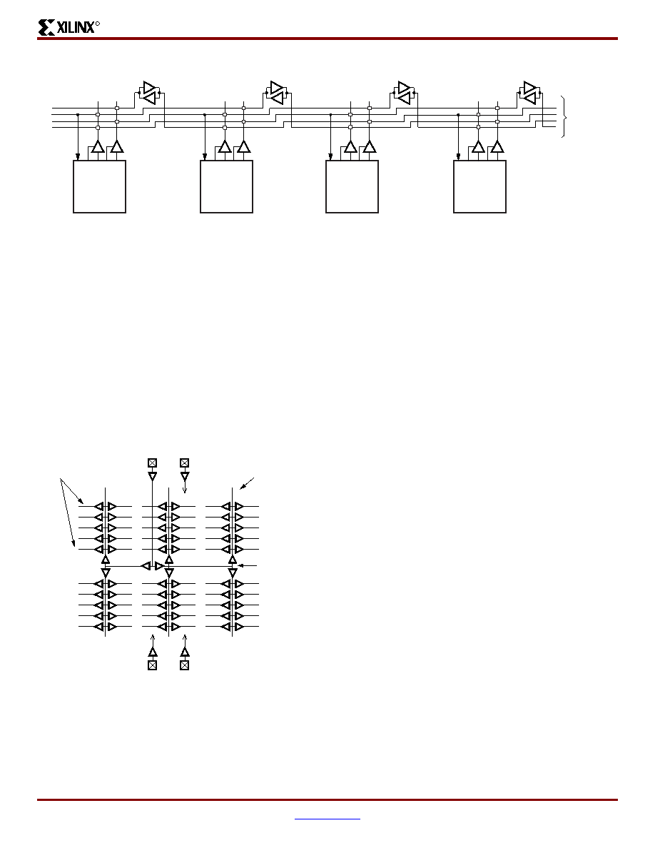
Figure 7: BUFT Connections to Dedicated Horizontal Bus Lines
CLB
3-State
Lines
DS001_07_090600
Figure 8: Global Clock Distribution Network
Global Clock
Spine
Global Clock
Column
GCLKPAD2
GCLKBUF2
GCLKPAD3
GCLKBUF3
GCLKBUF1
GCLKPAD1
GCLKBUF0
GCLKPAD0
Global
Clock Rows
DS001_08_060100
相關(guān)PDF資料 |
PDF描述 |
|---|---|
| GBM06DRKN-S13 | CONN EDGECARD 12POS .156 EXTEND |
| VI-21J-EU | CONVERTER MOD DC/DC 36V 200W |
| LQG15HS56NJ02D | INDUCTOR 56NH 200MA 0402 |
| GBM06DRKH-S13 | CONN EDGECARD 12POS .156 EXTEND |
| ADSP-BF531SBB400 | IC DSP CTLR 16BIT 400MHZ 169-BGA |
相關(guān)代理商/技術(shù)參數(shù) |
參數(shù)描述 |
|---|---|
| XC2S100-5FG456I | 功能描述:IC FPGA 2.5V I-TEMP 456-FBGA RoHS:否 類別:集成電路 (IC) >> 嵌入式 - FPGA(現(xiàn)場可編程門陣列) 系列:Spartan®-II 產(chǎn)品變化通告:XC4000(E,L) Discontinuation 01/April/2002 標(biāo)準(zhǔn)包裝:24 系列:XC4000E/X LAB/CLB數(shù):100 邏輯元件/單元數(shù):238 RAM 位總計(jì):3200 輸入/輸出數(shù):80 門數(shù):3000 電源電壓:4.5 V ~ 5.5 V 安裝類型:表面貼裝 工作溫度:-40°C ~ 100°C 封裝/外殼:120-BCBGA 供應(yīng)商設(shè)備封裝:120-CPGA(34.55x34.55) |
| XC2S100-5FGG256C | 功能描述:IC SPARTAN-II FPGA 100K 256-FBGA RoHS:是 類別:集成電路 (IC) >> 嵌入式 - FPGA(現(xiàn)場可編程門陣列) 系列:Spartan®-II 標(biāo)準(zhǔn)包裝:40 系列:Spartan® 6 LX LAB/CLB數(shù):3411 邏輯元件/單元數(shù):43661 RAM 位總計(jì):2138112 輸入/輸出數(shù):358 門數(shù):- 電源電壓:1.14 V ~ 1.26 V 安裝類型:表面貼裝 工作溫度:-40°C ~ 100°C 封裝/外殼:676-BGA 供應(yīng)商設(shè)備封裝:676-FBGA(27x27) |
| XC2S100-5FGG256I | 功能描述:IC SPARTAN-II FPGA 100K 256-FBGA RoHS:是 類別:集成電路 (IC) >> 嵌入式 - FPGA(現(xiàn)場可編程門陣列) 系列:Spartan®-II 標(biāo)準(zhǔn)包裝:40 系列:Spartan® 6 LX LAB/CLB數(shù):3411 邏輯元件/單元數(shù):43661 RAM 位總計(jì):2138112 輸入/輸出數(shù):358 門數(shù):- 電源電壓:1.14 V ~ 1.26 V 安裝類型:表面貼裝 工作溫度:-40°C ~ 100°C 封裝/外殼:676-BGA 供應(yīng)商設(shè)備封裝:676-FBGA(27x27) |
| XC2S100-5FGG456C | 制造商:XILINX 制造商全稱:XILINX 功能描述:Spartan-II FPGA Family |
| XC2S100-5FGG456I | 制造商:XILINX 制造商全稱:XILINX 功能描述:Spartan-II FPGA Family |
發(fā)布緊急采購,3分鐘左右您將得到回復(fù)。