- 您現(xiàn)在的位置:買賣IC網(wǎng) > PDF目錄372541 > XA-SCC (NXP Semiconductors N.V.) CMOS 16-bit communications microcontroller PDF資料下載
參數(shù)資料
| 型號(hào): | XA-SCC |
| 廠商: | NXP Semiconductors N.V. |
| 英文描述: | CMOS 16-bit communications microcontroller |
| 中文描述: | 的CMOS 16位微控制器的通信 |
| 文件頁(yè)數(shù): | 15/42頁(yè) |
| 文件大小: | 229K |
| 代理商: | XA-SCC |
第1頁(yè)第2頁(yè)第3頁(yè)第4頁(yè)第5頁(yè)第6頁(yè)第7頁(yè)第8頁(yè)第9頁(yè)第10頁(yè)第11頁(yè)第12頁(yè)第13頁(yè)第14頁(yè)當(dāng)前第15頁(yè)第16頁(yè)第17頁(yè)第18頁(yè)第19頁(yè)第20頁(yè)第21頁(yè)第22頁(yè)第23頁(yè)第24頁(yè)第25頁(yè)第26頁(yè)第27頁(yè)第28頁(yè)第29頁(yè)第30頁(yè)第31頁(yè)第32頁(yè)第33頁(yè)第34頁(yè)第35頁(yè)第36頁(yè)第37頁(yè)第38頁(yè)第39頁(yè)第40頁(yè)第41頁(yè)第42頁(yè)
Philips Semiconductors
Preliminary specification
XA-SCC
CMOS 16-bit communications microcontroller
1999 Mar 29
15
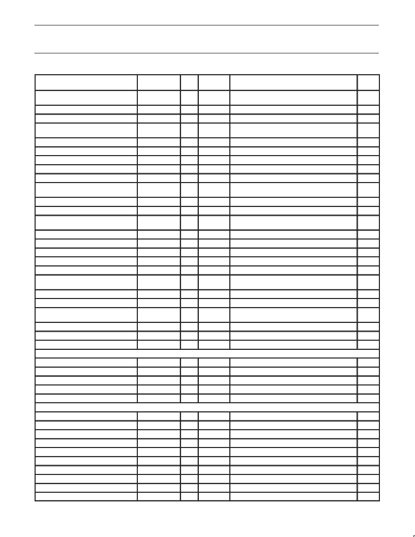
MMR Name
Reset
Value
Description
Address
Offset
Size
Read/Write or
Read Only
Buffer Base Register Ch.1 Tx
R/W
8
154h
Wrap Reload Value for A15–A8, A7–A0 reloaded
to zero by hardware
Upper Bound (plus 1) on A15–A0
Current Address pointer A15–A0
Corresponds to A15–A0 Byte Count, generates
interrupt if enabled and byte count exceeded.
Byte0 & 1
Byte2 & 3
Control Register
Control & Status Register
Points to 64K data segment
Wrap Reload Value for A15 –A8, A7–A0 reloaded
to zero by hardware
Upper Bound (plus 1) on A15–A0
Current Address pointer A15–A0
Corresponds to A15–A0 Byte Count, generates
interrupt if enabled and byte count exceeded.
Byte0 & 1
Byte2 & 3
Control Register
Control & Status Register
Points to 64K data segment
Wrap Reload Value for A15 –A8
A7–A0 reloaded to zero by hardware
Upper Bound (plus 1) on A15–A0
Current Address pointer A15–A0
Corresponds to A15–A0 Byte Count, generates
interrupt if enabled and byte count exceeded.
Byte0 & 1
Byte2 & 3
RESERVED for future DMA
00h
Buffer Bound Register Ch.1 Tx
Address Pointer Reg Ch.1 Tx
Byte Count Register Ch.1 Tx
R/W
R/W
R/W
16
16
16
156h
158h
15Ah
0000h
0000h
0000h
Data FIFO Register Ch.1 Lo Tx
Data FIFO Register Ch.1 Hi Tx
DMA Control Register Ch.2 Tx
FIFO Control & Status Register Ch.2 Tx
Segment Register Ch.2 Tx
Buffer Base Register Ch.2 Tx
R/W
R/W
R/W
R/W
R/W
R/W
16
16
8
8
8
8
15Ch
15Eh
160h
161h
162h
164h
0000h
0000h
00h
00h
00h
00h
Buffer Bound Register Ch.2 Tx
Address Pointer Reg Ch.2 Tx
Byte Count Register Ch.2 Tx
R/W
R/W
R/W
16
16
16
166h
168h
16Ah
0000h
0000h
0000h
Data FIFO Register Ch.2 Lo Tx
Data FIFO Register Ch.2 Hi Tx
DMA Control Register Ch.3 Tx
FIFO Control & Status Register Ch.3 Tx
Segment Register Ch. 3 Tx
Buffer Base Register Ch. 3 Tx
R/W
R/W
R/W
R/W
R/W
R/W
16
16
8
8
8
8
16Ch
16Eh
170h
171h
172h
174h
0000h
0000h
00h
00h
00h
00h
Buffer Bound Register Ch.3 Tx
Address Pointer Reg Ch.3 Tx
Byte Count Register Ch.3 Tx
R/W
R/W
R/W
16
16
16
176h
178h
17Ah
0000h
0000h
0000h
Data FIFO Register Ch.3Lo Tx
Data FIFO Register Ch.3 Hi Tx
R/W
R/W
R/W
16
16
17Ch
17Eh
180–1FEh
0000h
0000h
—
Miscellaneous DMA Registers
8
8
8
8
16
V.54/2047 Registers
8
8
8
8
8
8
8
8
8
8
Rx Character Time Out Register Ch.0
Rx Character Time Out Register Ch.1
Rx Character Time Out Register Ch.2
Rx Character Time Out Register Ch.3
Global DMA Interrupt Register
R/W
R/W
R/W
R/W
R/W
200h
202h
204h
206h
210h
0 value disables counter interrupt.
Same as above, for Rx1
Same as above, for Rx2
Same as above, for Rx3
DMA Interrupt Flags
00h
00h
00h
00h
0000h
VACS
VACFG
VATCL
VATCH
VAEC
VBCS
VBCFG
VBTCL
VBTCH
VBEC
R/W
R/W
R/W
R/W
R/W
R/W
R/W
R/W
R/W
R/W
240h
241h
242h
243h
244h
248h
249h
24Ah
24Bh
24Ch
V.54 2047 Unit A Control & Status
V.54 2047 Unit A Configuration
V.54 2047 Unit A Threshold Cntr Lo
V.54 2047 Unit A Threshold Cntr Hi
V.54 2047 Unit A Error Counter
V.54 2047 Unit B Control & Status
V.54 2047 Unit B Configuration
V.54 2047 Unit B Threshold Cntr Lo
V.54 2047 Unit B Threshold Cntr Hi
V.54 2047 Unit B Error Counter
00h
—
—
—
—
00h
—
—
—
—
相關(guān)PDF資料 |
PDF描述 |
|---|---|
| XA1024 | Temperature Sensor(Frequencies Range Between 2 And 30 MHz)(溫度傳感器(頻率范圍: 2至 30 MHz)) |
| XA979 | Temperature Sensor(Frequencies Range Between 2 And 30 MHz)(溫度傳感器(頻率范圍: 2至 30 MHz)) |
| XAG30 | XA 16-bit microcontroller family 32K/512 OTP/ROM/ROMless, watchdog, 2 UARTs |
| XAM1214-130 | RF POWER TRANSISTORS L-BAND RADAR APPLICATIONS |
| XB0ASB03A1BR | SCHOTTKY BARRIER DIODE 500MA 30V TYPE |
相關(guān)代理商/技術(shù)參數(shù) |
參數(shù)描述 |
|---|---|
| XA-SK-AUDIO | 制造商:XMOS Ltd 功能描述:SLICEKIT AUDIO SLICE CARD |
| XA-SK-E100 | 制造商:XMOS Ltd 功能描述:10/100 ETHERNET SLICE CARD |
| XA-SK-GPIO | 制造商:XMOS Ltd 功能描述:GPIO SLICE CARD |
| XA-SK-ISBUS | 制造商:XMOS Ltd 功能描述:INDUSTRIAL SLICE CARD |
| XA-SK-SCR480 | 制造商:XMOS Ltd 功能描述:DISPLAY SLICE CARD |
發(fā)布緊急采購(gòu),3分鐘左右您將得到回復(fù)。