- 您現(xiàn)在的位置:買賣IC網(wǎng) > PDF目錄372541 > XA-SCC (NXP Semiconductors N.V.) CMOS 16-bit communications microcontroller PDF資料下載
參數(shù)資料
| 型號: | XA-SCC |
| 廠商: | NXP Semiconductors N.V. |
| 英文描述: | CMOS 16-bit communications microcontroller |
| 中文描述: | 的CMOS 16位微控制器的通信 |
| 文件頁數(shù): | 13/42頁 |
| 文件大?。?/td> | 229K |
| 代理商: | XA-SCC |
第1頁第2頁第3頁第4頁第5頁第6頁第7頁第8頁第9頁第10頁第11頁第12頁當(dāng)前第13頁第14頁第15頁第16頁第17頁第18頁第19頁第20頁第21頁第22頁第23頁第24頁第25頁第26頁第27頁第28頁第29頁第30頁第31頁第32頁第33頁第34頁第35頁第36頁第37頁第38頁第39頁第40頁第41頁第42頁
Philips Semiconductors
Preliminary specification
XA-SCC
CMOS 16-bit communications microcontroller
1999 Mar 29
13
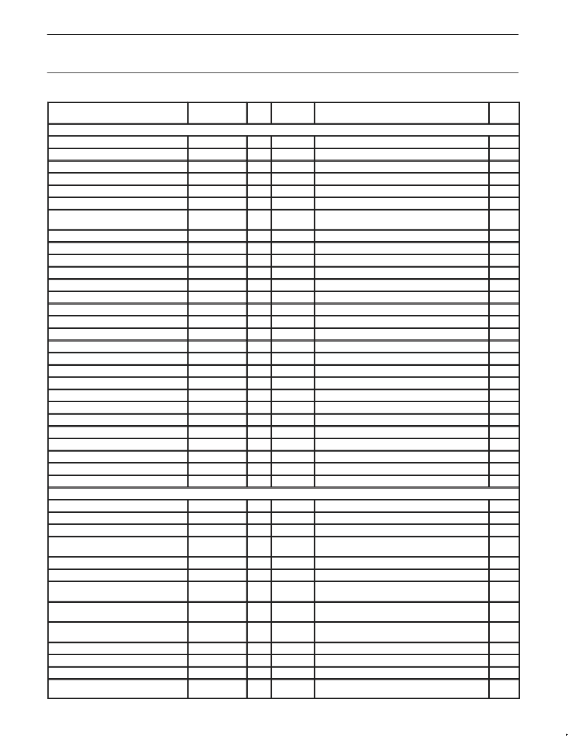
MMR Name
Reset
Value
Description
Address
Offset
Size
Read/Write or
Read Only
SCC3 Registers
8
8
8
8
8
8
8CAh
8
8CCh
SCC3 Write Register 0
SCC3 Write Register 1
SCC3 Write Register 2
SCC3 Write Register 3
SCC3 Write Register 4
SCC3 Write Register 5
SCC3 Write Register 6
R/W
R/W
R/W
R/W
R/W
R/W
R/W
8C0h
8C2h
8C4h
8C6h
8C8h
Command register
Tx/Rx Interrupt & data transfer mode
Extended Features Control
Receive Parameter and Control
Tx/Rx misc. parameters & mode
Tx. parameter and control
Sync character or SDLC address field or Match
Character 0
Sync character or SDLC flag or Match Character 1
Transmit Data Buffer
Master Interrupt control
Misc. Tx/Rx control register
Clock Mode Control
Lower Byte of Baud rate time constant
Upper Byte of Baud rate time constant
Misc. Control bits
External/Status interrupt control
Match Character 2 (wr16)
Match Character 3 (wr17)
Tx/Rx buffer and external status
Receive condition status/residue code
00h
xx
xx
00h
00h
00h
00h
SCC3 Write Register 7
SCC3 Write Register 8
SCC3 Write Register 9
SCC3 Write Register 10
SCC3 Write Register 11
SCC3 Write Register 12
SCC3 Write Register 13
SCC3 Write Register 14
SCC3 Write Register 15
SCC3 Write Register 16
SCC3 Write Register 17
SCC3 Read Register 0
SCC3 Read Register 1
Reserved
SCC3 Read Register 3
SCC3 Read Register 6
SCC3 Read Register 7
SCC3 Read Register 8
Reserved
SCC3 Read Register 10
Reserved
R/W
R/W
R/W
R/W
R/W
R/W
R/W
R/W
R/W
R/W
R/W
RO
RO
8
8
8
8
8
8
8
8
8
8
8
8
8
8CEh
8D0h
8D2h
8D4h
8D6h
8D8h
8DAh
8DCh
8DEh
8E8h
8EAh
8E0h
8E2h
8E4h
8E6h
8ECh
8EEh
8F0h
8F2h
8F4h
8F6–8FEh
xx
xx
xx
00h
xx
00h
00h
xx
f8h
00h
00h
—
—
—
—
—
—
—
—
—
—
RO
RO
RO
RO
8
8
8
8
Interrupt Pending Register
SDLC byte count low register
SDLC byte count high & FIFO status
Receive Buffer
RO
8
Loop/clock status
Rx DMA Registers
8
8
8
8
DMA Control Register Ch.0 Rx
FIFO Control & Status Reg Ch.0 Rx
Segment Register Ch.0 Rx
Buffer Base Register Ch.0 Rx
R/W
R/W
R/W
R/W
100h
101h
102h
104h
Control Register
Control & Status Register
Points to 64K data segment
Wrap Reload Value for A15 –A8, A7–A0 reloaded
to zero by hardware
Upper Bound (plus 1) on A15–A0
Current Address pointer A15–A0
Corresponds to A15–A0 Byte Count, generates
interrupt if enabled and byte count exceeded.
10Ch = Byte 0 = older,
10Dh = Byte 1 = younger
10Eh = Byte 2 = older,
10Fh = Byte 3 = younger
Control Register
Control & Status Register
Points to 64K data segment
Wrap Reload Value for A15 –A8, A7–A0 reloaded
to zero by hardware
00h
00h
00h
00h
Buffer Bound Register Ch.0 Rx
Address Pointer Reg Ch.0 Rx
Byte Count Register Ch.0 Rx
R/W
R/W
R/W
16
16
16
106h
108h
10Ah
0000h
0000h
0000h
Data FIFO Register Ch.0 Lo Rx
R/W
16
10Ch
00h
00h
00h
00h
00h
00h
00h
00h
Data FIFO Register Ch.0 Hi Rx
R/W
16
10Eh
DMA Control Register Ch.1 Rx
FIFO Control & Status Register Ch.1 Rx
Segment Register Ch. 1 Rx
Buffer Base Register Ch. 1 Rx
R/W
R/W
R/W
R/W
8
8
8
8
110h
111h
112h
114h
相關(guān)PDF資料 |
PDF描述 |
|---|---|
| XA1024 | Temperature Sensor(Frequencies Range Between 2 And 30 MHz)(溫度傳感器(頻率范圍: 2至 30 MHz)) |
| XA979 | Temperature Sensor(Frequencies Range Between 2 And 30 MHz)(溫度傳感器(頻率范圍: 2至 30 MHz)) |
| XAG30 | XA 16-bit microcontroller family 32K/512 OTP/ROM/ROMless, watchdog, 2 UARTs |
| XAM1214-130 | RF POWER TRANSISTORS L-BAND RADAR APPLICATIONS |
| XB0ASB03A1BR | SCHOTTKY BARRIER DIODE 500MA 30V TYPE |
相關(guān)代理商/技術(shù)參數(shù) |
參數(shù)描述 |
|---|---|
| XA-SK-AUDIO | 制造商:XMOS Ltd 功能描述:SLICEKIT AUDIO SLICE CARD |
| XA-SK-E100 | 制造商:XMOS Ltd 功能描述:10/100 ETHERNET SLICE CARD |
| XA-SK-GPIO | 制造商:XMOS Ltd 功能描述:GPIO SLICE CARD |
| XA-SK-ISBUS | 制造商:XMOS Ltd 功能描述:INDUSTRIAL SLICE CARD |
| XA-SK-SCR480 | 制造商:XMOS Ltd 功能描述:DISPLAY SLICE CARD |
發(fā)布緊急采購,3分鐘左右您將得到回復(fù)。