- 您現(xiàn)在的位置:買賣IC網(wǎng) > PDF目錄361880 > WM8191 (Wolfson Microelectronics) TVS BI-DIR 6.0V 400W SMA PDF資料下載
參數(shù)資料
| 型號(hào): | WM8191 |
| 廠商: | Wolfson Microelectronics |
| 英文描述: | TVS BI-DIR 6.0V 400W SMA |
| 中文描述: | 14位6MSPS獨(dú)聯(lián)體/防治荒漠化公約模擬前端/數(shù)字轉(zhuǎn)換器 |
| 文件頁(yè)數(shù): | 13/27頁(yè) |
| 文件大?。?/td> | 355K |
| 代理商: | WM8191 |
第1頁(yè)第2頁(yè)第3頁(yè)第4頁(yè)第5頁(yè)第6頁(yè)第7頁(yè)第8頁(yè)第9頁(yè)第10頁(yè)第11頁(yè)第12頁(yè)當(dāng)前第13頁(yè)第14頁(yè)第15頁(yè)第16頁(yè)第17頁(yè)第18頁(yè)第19頁(yè)第20頁(yè)第21頁(yè)第22頁(yè)第23頁(yè)第24頁(yè)第25頁(yè)第26頁(yè)第27頁(yè)
Advanced Information
WM8191
WOLFSON MICROELECTRONICS LTD
AI Rev 3.1 April 2001
13
MCLK
VSMP
VS
R
S
/CL (CDSREF = 00)
R
S
/CL (CDSREF = 01)
R
S
/CL (CDSREF = 10)
R
S
/CL (CDSREF = 11)
Figure 10 Reset Sample and Clamp Timing
For CIS type sensor signals, non-CDS processing is used. In this case, the video level is processed
with respect to the voltage on pin VRLC/VBIAS, generated internally or externally as described
above. The VRLC/VBIAS pin is sampled by R
s
at the same time as V
s
samples the video level in
this mode.
OFFSET ADJUST AND PROGRAMMABLE GAIN
The output from the CDS block is a differential signal, which is added to the output of an 8-bit offset
DAC to compensate for offsets and then amplified by an 8-bit PGA. The gain and offset for each
channel are independently programmable by writing to control bits DAC[7:0] and PGA[7:0].
In colour line-by-line mode the gain and offset coefficients for each colour can be multiplexed in order
(Red
→
Green
→
Blue
→
Red
…
) by pulsing the ACYC/RLC pin, or controlled via the FME,
ACYCNRLC and INTM[1:0] bits. Refer to the Line-by-Line Operation section for more details.
ADC INPUT BLACK LEVEL ADJUST
The output from the PGA must be offset to match the full-scale range of the ADC. For negative-going
input signals, a black level (zero differential) output from the PGA should be offset to the top of the
ADC range. For positive going input signal the black level should be offset to the bottom of the ADC
range. This is achieved by writing to control bits PGAFS[1:0].
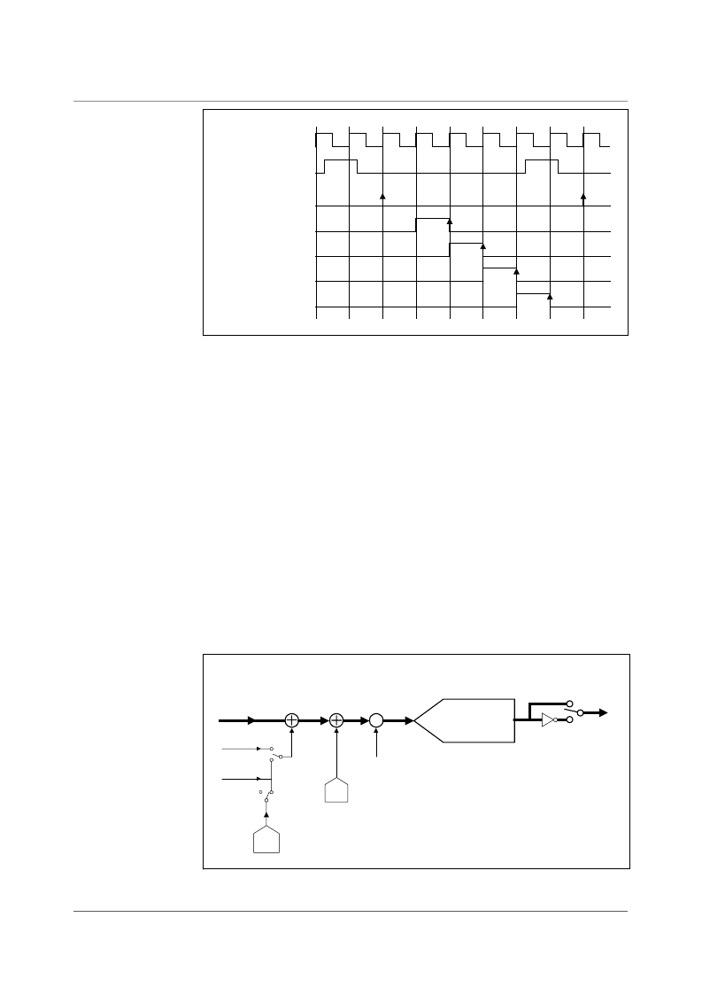
OVERALL SIGNAL FLOW SUMMARY
Figure 11 represents the processing of the video signal through the WM8191.
V
RESET
V
VRLC
V
3
CDS = 1
CDS = 0
RLCEXT=1
260mV*(DAC[7:0]-127.5)/127.5
analog
-
X
++
V
RLCSTEP
*RLCV[3:0] + V
RLCBOT
OP[13:0]
D
1
digital
ADC BLOCK
PGA
BLOCK
OFFSET DAC
BLOCK
V
1
INPUT
SAMPLING
BLOCK
D
2
CDS, RLCEXT,RLCV[3:0], DAC[7:0],
PGA[7:0], PGAFS[1:0] and INVOP are set
by programming internal control registers.
CDS = 1 for CDS, 0 for non-CDS
V
IN
is RINP or GINP or BINP
V
RESET
is V
sampled during reset clamp
V
VRLC
is voltage applied to VRLC pin
V
IN
x (16383/V
)
+0 if PGAFS[1:0]=11
+16383 if PGAFS[1:0]=10
+8191 if PGAFS[1:0]=0x
PGA gain
A = 208/(283-PGA[7:0])
OUTPUT
INVERT
BLOCK
D2 = D1 if INVOP = 0
D2 = 16383-D1 if INVOP = 1
Offset
DAC
RLC
DAC
+
V
2
RLCEXT=0
Figure 11 Overall Signal Flow
相關(guān)PDF資料 |
PDF描述 |
|---|---|
| WM8192 | TVS UNIDIRECT 400W 6.5V SMA |
| WM8196 | (8+8)BIT OUTPUT 16-BIT CIS/CCD AFE/DIGITISER |
| WM8199 | 20MSPS 16-bit CCD Digitiser |
| WM8199CDR | TVS BIDIRECT 400W 60V SMA |
| WM8199CDS | TVS UNIDIRECT 400W 64V SMA |
相關(guān)代理商/技術(shù)參數(shù) |
參數(shù)描述 |
|---|---|
| WM8192 | 制造商:WOLFSON 制造商全稱:WOLFSON 功能描述:(8+8) Bit Output 16-bit CIS/CCD AFE/Digitiser |
| WM8195 | 制造商:WOLFSON 制造商全稱:WOLFSON 功能描述:14-bit 12MSPS CIS/CCD Analogue Front End/Digitiser |
| WM8195_05 | 制造商:WOLFSON 制造商全稱:WOLFSON 功能描述:14-bit 12MSPS CIS/CCD Analogue Front End/Digitiser |
| WM8195SCFT/RV | 功能描述:模數(shù)轉(zhuǎn)換器 - ADC 14Bit 12MSPS 3C AFE RoHS:否 制造商:Texas Instruments 通道數(shù)量:2 結(jié)構(gòu):Sigma-Delta 轉(zhuǎn)換速率:125 SPs to 8 KSPs 分辨率:24 bit 輸入類型:Differential 信噪比:107 dB 接口類型:SPI 工作電源電壓:1.7 V to 3.6 V, 2.7 V to 5.25 V 最大工作溫度:+ 85 C 安裝風(fēng)格:SMD/SMT 封裝 / 箱體:VQFN-32 |
| WM8195SCFT/V | 功能描述:模數(shù)轉(zhuǎn)換器 - ADC 14Bit 12MSPS 3Ch AFE RoHS:否 制造商:Texas Instruments 通道數(shù)量:2 結(jié)構(gòu):Sigma-Delta 轉(zhuǎn)換速率:125 SPs to 8 KSPs 分辨率:24 bit 輸入類型:Differential 信噪比:107 dB 接口類型:SPI 工作電源電壓:1.7 V to 3.6 V, 2.7 V to 5.25 V 最大工作溫度:+ 85 C 安裝風(fēng)格:SMD/SMT 封裝 / 箱體:VQFN-32 |
發(fā)布緊急采購(gòu),3分鐘左右您將得到回復(fù)。