- 您現(xiàn)在的位置:買賣IC網(wǎng) > PDF目錄140360 > WEDPN8M64V-133B2C (MICROSEMI CORP-PMG MICROELECTRONICS) 8M X 64 SYNCHRONOUS DRAM, 5.5 ns, PBGA219 PDF資料下載
參數(shù)資料
| 型號: | WEDPN8M64V-133B2C |
| 廠商: | MICROSEMI CORP-PMG MICROELECTRONICS |
| 元件分類: | DRAM |
| 英文描述: | 8M X 64 SYNCHRONOUS DRAM, 5.5 ns, PBGA219 |
| 封裝: | 21 X 21 MM, PLASTIC, BGA-219 |
| 文件頁數(shù): | 1/15頁 |
| 文件大小: | 398K |
| 代理商: | WEDPN8M64V-133B2C |
WEDPN8M64V-XB2X
1
White Electronic Designs Corporation (602) 437-1520 www.whiteedc.com
White Electronic Designs
January 2005
Rev. 2
GENERAL DESCRIPTION
The 64MByte (512Mb) SDRAM is a high-speed CMOS,
dynamic random-access memory using 4 chips containing
134,217,728 bits. Each chip is internally congured as a
quad-bank DRAM with a synchronous interface. Each of
the chip’s 33,554,432-bit banks is organized as 4,096 rows
by 512 columns by 16 bits.
Read and write accesses to the SDRAM are burst oriented;
accesses start at a selected location and continue for
a programmed number of locations in a programmed
sequence. Accesses begin with the registration of an
ACTIVE command, which is then followed by a READ or
WRITE command. The address bits registered coincident
with the ACTIVE command are used to select the bank
and row to be accessed (BA0, BA1 select the bank; A0-
11 select the row). The address bits registered coincident
with the READ or WRITE command are used to select the
starting column location for the burst access.
The SDRAM provides for programmable READ or WRITE
burst lengths of 1, 2, 4 or 8 locations, or the full page, with
a burst terminate option. An AUTO PRECHARGE function
may be enabled to provide a self-timed row precharge that
is initiated at the end of the burst sequence.
The 512Mb SDRAM uses an internal pipelined architecture
to achieve high-speed operation. This architecture is
compatible with the 2n rule of prefetch architectures, but
it also allows the column address to be changed on every
clock cycle to achieve a high-speed, fully random access.
Precharging one bank while accessing one of the other
three banks will hide the precharge cycles and provide
seamless, high-speed, random-access operation.
8Mx64 Synchronous DRAM
FEATURES
High Frequency = 100, 125, 133MHz
Package:
219 Plastic Ball Grid Array (PBGA), 21 x 21mm
Single 3.3V ±0.3V power supply
Unbuffered
Fully synchronous; all signals registered on positive edge of
system clock cycle
Internal pipelined operation; column address can be changed
every clock cycle
Internal banks for hiding row access/precharge
Programmable Burst length 1,2,4,8 or full page
4,096 refresh cycles
Commercial, Industrial and Military Temperature Ranges
Organized as 8M x 64
User Congurable as 2 x 8M x 32 or
4 x 8M x 16
Weight: WEDPN8M64V-XB2X - 2 grams typical
BENEFITS
58% SPACE SAVINGS
Reduced part count
Reduced trace lengths for lower parasitic capacitance
Laminate interposer for optimum TCE match
Suitable for hi-reliability applications
Upgradeable to 16M x 64 density (WEDPN16M64V-XB2X)
* This product is subject to change without notice.
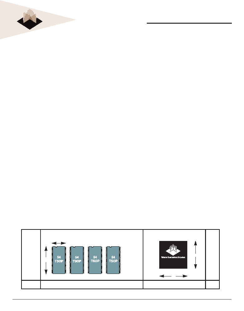
21
Discrete Approach
S
A
V
I
N
G
S
Area
4 x 265mm2= 1060mm2
441mm2
58%
ACTUAL SIZE
22.3
11.9
21
WEDPN8M64V-XB2X
相關PDF資料 |
PDF描述 |
|---|---|
| WMF2M8-120LM5 | 2M X 8 FLASH 5V PROM, 120 ns, CQCC44 |
| WS128K32N-25H1I | 128K X 32 MULTI DEVICE SRAM MODULE, 25 ns, CPGA66 |
| WS128K32N-35H1CA | 128K X 32 MULTI DEVICE SRAM MODULE, 35 ns, CPGA66 |
| WS128K32L-15G2LMA | 128K X 32 MULTI DEVICE SRAM MODULE, 15 ns, CQFP68 |
| WS128K32N-45G2TMEA | 128K X 32 MULTI DEVICE SRAM MODULE, 45 ns, CQFP68 |
相關代理商/技術參數(shù) |
參數(shù)描述 |
|---|---|
| WEDPN8M64V-133B2I | 制造商:WEDC 制造商全稱:White Electronic Designs Corporation 功能描述:8Mx64 Synchronous DRAM |
| WEDPN8M64V-133B2M | 制造商:WEDC 制造商全稱:White Electronic Designs Corporation 功能描述:8Mx64 Synchronous DRAM |
| WEDPN8M64V-133BC | 制造商:Microsemi Corporation 功能描述:8M X 64 SDRAM MODULE, 3.3V, 133 MHZ, 219 PBGA 25MM X 25MM, C - Bulk |
| WEDPN8M64VR-XBX | 制造商:未知廠家 制造商全稱:未知廠家 功能描述:Registered SDRAM MCP |
| WEDPN8M64V-XB2X | 制造商:WEDC 制造商全稱:White Electronic Designs Corporation 功能描述:8Mx64 Synchronous DRAM |
發(fā)布緊急采購,3分鐘左右您將得到回復。