- 您現(xiàn)在的位置:買賣IC網(wǎng) > PDF目錄203637 > W9751G8JB-18 (WINBOND ELECTRONICS CORP) DDR DRAM, PBGA84 PDF資料下載
參數(shù)資料
| 型號: | W9751G8JB-18 |
| 廠商: | WINBOND ELECTRONICS CORP |
| 元件分類: | DRAM |
| 英文描述: | DDR DRAM, PBGA84 |
| 封裝: | 8 X 12.50 MM, ROHS COMPLIANT, WBGA-84 |
| 文件頁數(shù): | 3/17頁 |
| 文件大小: | 1458K |
| 代理商: | W9751G8JB-18 |
11/16
2) Cross-conduction protection circuit
In the full bridge output stage, when the upper and lower transistors are turned on at the same time, and this condition
exists during the period of transition from high to low, or low to high, a rush current flows from the power supply to
ground, resulting in a loss. This circuit protects against the rush current by providing a dead time (about 400ns,
nominal) at the transition.
3) Output protection circuits
a) Under voltage lock out (UVLO) circuit
To secure the lowest power supply voltage necessary to operate the controller, and to prevent under voltage
malfunctions, a UVLO circuit has been built into this driver. When the power supply voltage falls to 5.0V (nominal)
or below, the controller forces all driver outputs to high impedance. When the voltage rises to 5.5V (nominal) or
above, the UVLO circuit ends the lockout operation and returns the chip to normal operation.
b) Over voltage protection (OVP) circuit
When the power supply voltage exceeds 47V (nominal), the controller forces all driver outputs to high impedance.
The OVP circuit is released and its operation ends when the voltage drops back to 43V (nominal) or below. This
protection circuit does not work in the stand-by mode. Also, note that this circuit is supplementary, and thus if it is
asserted, the absolute maximum rating will have been exceeded. Therefore, do not continue to use the IC after this
circuit is activated, and do not operate the IC in an environment where activation of the circuit is assumed.
c) Thermal shutdown (TSD) circuit
The TSD circuit operates when the junction temperature of the driver exceeds the preset temperature (175°C
nominal). At this time, the controller forces all driver outputs to high impedance. Since thermal hysteresis is
provided in the TSD circuit, the chip returns to normal operation when the junction temperature falls below the
preset temperature (150°C nominal). Thus, it is a self-returning type circuit.
The TSD circuit is designed only to shut the IC off to prevent thermal runaway. It is not designed to protect the IC or
guarantee its operation in the presence of extreme heat. Do not continue to use the IC after the TSD circuit is
activated, and do not operate the IC in an environment where activation of the circuit is assumed.
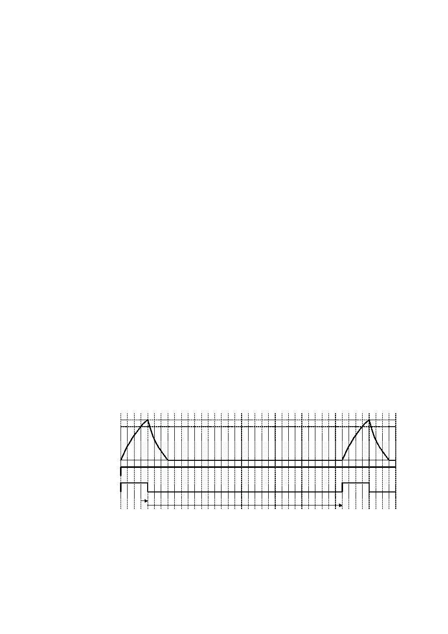
d) Over current protection (OCP) circuit
To protect this driver IC from ground faults, power supply line faults and load short circuits, the OCP circuit
monitors the output current for the circuit’s monitoring time (10μs, nominal). When the protection circuit detects an
over current, the controller forces all driver outputs to high impedance during the off time (290μs, nominal). The IC
returns to normal operation after the off time period has elapsed (self-returning type). At the two channels type, this
circuit works independently for each channel.
Fig.42 Over current protection (timing chart)
Threshold
Iout
CTRL Input
Internal status
Monitor / Timer
0
OFF
ON
mon.
off timer
ON
相關(guān)PDF資料 |
PDF描述 |
|---|---|
| W9812G21H-6I | 4M X 32 SYNCHRONOUS DRAM, 5 ns, PDSO86 |
| W9812G21H-6C | 4M X 32 SYNCHRONOUS DRAM, 4.5 ns, PDSO86 |
| W9812G6JH-6 | 8M X 16 SYNCHRONOUS DRAM, 5 ns, PDSO54 |
| W986416AH-10 | 4M X 16 SYNCHRONOUS DRAM, 8 ns, PDSO54 |
| W986432DH-6 | 2M X 32 SYNCHRONOUS DRAM, 5 ns, PDSO86 |
相關(guān)代理商/技術(shù)參數(shù) |
參數(shù)描述 |
|---|---|
| W9751G8KB-25 | 制造商:Winbond Electronics Corp 功能描述:IC DDR2 SDRAM 512MBIT 2.5NS 制造商:Winbond Electronics Corp 功能描述:IC DDR2 SDRAM 512MBIT 2.5NS BGA |
| W979H2KBQX2I | 制造商:Winbond Electronics Corp 功能描述: 制造商:Winbond Electronics Corp 功能描述:512MB LPDDR2, X32, 400MHZ, -40 |
| W97ACPX-1 | 制造商:Struthers-Dunn 功能描述: |
| W97ACPX-2 | 制造商:Magnecraft 功能描述:Electromechanical Relay DPDT-DB/DPDT-DM 25A 24VAC Plug-In 制造商:Struthers-Dunn 功能描述:Electromechanical Relay DPDT-DB/DPDT-DM 25A 24VAC Plug-In |
| W97ACPX-3 | 制造商:Struthers-Dunn 功能描述: |
發(fā)布緊急采購,3分鐘左右您將得到回復(fù)。