- 您現(xiàn)在的位置:買賣IC網(wǎng) > PDF目錄203632 > W78M64110SBC (WHITE ELECTRONIC DESIGNS CORP) 8M X 64 FLASH 3.3V PROM, 110 ns, PBGA159 PDF資料下載
參數(shù)資料
| 型號: | W78M64110SBC |
| 廠商: | WHITE ELECTRONIC DESIGNS CORP |
| 元件分類: | PROM |
| 英文描述: | 8M X 64 FLASH 3.3V PROM, 110 ns, PBGA159 |
| 封裝: | 13 X 22 MM, 1.27 MM PITCH, PLASTIC, BGA-159 |
| 文件頁數(shù): | 24/50頁 |
| 文件大小: | 1679K |
| 代理商: | W78M64110SBC |
第1頁第2頁第3頁第4頁第5頁第6頁第7頁第8頁第9頁第10頁第11頁第12頁第13頁第14頁第15頁第16頁第17頁第18頁第19頁第20頁第21頁第22頁第23頁當前第24頁第25頁第26頁第27頁第28頁第29頁第30頁第31頁第32頁第33頁第34頁第35頁第36頁第37頁第38頁第39頁第40頁第41頁第42頁第43頁第44頁第45頁第46頁第47頁第48頁第49頁第50頁
30
White Electronic Designs Corporation (602) 437-1520 www.whiteedc.com
White Electronic Designs
W78M64VP-XSBX
November 2009
2010 White Electronic Designs Corp. All rights reserved
Rev. 10
White Electronic Designs Corp. reserves the right to change products or specications without notice.
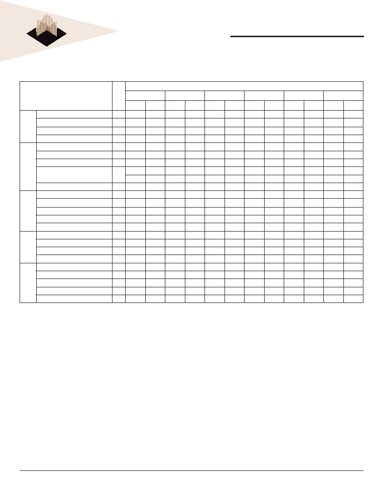
TABLE 40 SECTOR PROTECTION COMMAND DEFINITIONS
Command
Cycles
Bus Cycles (Note 1-5)
First
Second
Third
Fouth
Fifth
Sixth
Addr
Data
Addr
Data
Addr
Data
Addr
Data
Addr
Data
Addr
Data
Lock
Register
Command Set Entry
3
555
AA
2AA
55
555
Program (6)
2
XXX
A0
XXX
DATA
Read (6)
1
00
RD
Command Set Exit (7, 8)
2
XXX
90
XXX
00
Password
Command Set Entry
3
555
AA
2AA
55
555
Password Program (9)
2
XXX
A0
PWAx
PWDx
Password Read (10)
4
00
PWD0
01
PWD 1
02
PWD 2
03
PWD 3
Password Unlock (10)
7
00
25
00
03
00
PWD 0
01
PWD 1
02
PWD 2
03
PWD 3
00
29
Command Set Exit (7, 8)
2
XXX
90
XXX
00
Global
Non-V
olatile
PPB Command Set Entry
3
555
AA
2AA
55
555
PPB Program (11, 12)
2
XXX
A0
SA
00
All PPB Erase (13)
2
XXX
80
00
30
PPB Status Read (12)
1
SA
RD (0)
PPB Command Set Exit (7, 8)
2
XXX
90
XXX
00
Global
V
olatile
Freeze
PPB Lock Command Set Entry
3
555
AA
2AA
55
555
PPB Lock Set (12)
2
XXX
A0
XXX
00
PPB Lock Command Set Exit (7, 8)
1
XXX
RD (0)
PPB Lock Command Set Exit (7, 8)
2
XXX
90
XXX
00
Volatile
DYB Command Set Entry
3
555
AA
2AA
55
555
DYB Set (11, 12)
2
XXX
A0
SA
00
DYB Clear (12)
2
XXX
A0
SA
01
DYB Status Read (12)
1
SA
RD (0)
DYB Command Set Exit (7, 8)
2
XXX
90
XXX
00
Legend
X = Don’t care
RD(0) = Read data.
SA = Sector Address. Address bits Amax–A16 uniquely select any sector.
Notes
1.
See Table 2 for description of bus operations.
2.
All values are in hexadecimal.
3.
All bus cycles are write cycles unless otherwise noted.
4.
Data bits DQ15-DQ8 are don’t cares for unlock and command cycles.
5.
Address bits AMAX:A16 are don’t cares for unlock and command cycles, unless SA
or PA required. (AMAX is the Highest Address pin.)
6.
All Lock Register bits are one-time programmable. Program state = “0” and the erase
state = “1.” The Persistent Protection Mode Lock Bit and the Password Protection
Mode Lock Bit cannot be programmed at the same time or the Lock Register Bits
Program operation aborts and returns the device to read mode. Lock Register bits
that are reserved for future use default to “1’s.” The Lock Register is shipped out as
PWD = Password
PWDx = Password word0, word1, word2, and word3.
Data = Lock Register Contents: PD(0) = Secured Silicon Sector Protection Bit,
PD(1) = Persistent Protection Mode Lock Bit, PD(2) = Password Protection Mode Lock Bit.
“FFFF’s” before Lock Register Bit program execution.
7.
The Exit command returns the device to reading the array.
8.
If any Command Set Entry command was written, an Exit command must be issued
to reset the device into read mode.
9.
For PWDx, only one portion of the password can be programmed per each “A0”
command.
10. Note that the password portion can be entered or read in any order as long as the
entire 64-bit password is entered or read.
11. If ACC = VHH, sector protection matches when ACC = VIH.
12. Protected State = “00h,” Unprotected State = “01h.”
13. The All PPB Erase command embeds programming of all PPB bits before erasure.
相關PDF資料 |
PDF描述 |
|---|---|
| W78M64V100SBC | 8M X 64 FLASH 3.3V PROM MODULE, 100 ns, PBGA159 |
| W78M64VP120SBM | SPECIALTY MEMORY CIRCUIT, PBGA156 |
| W78M64VP120SBI | SPECIALTY MEMORY CIRCUIT, PBGA156 |
| W83L761G | DIGITAL TEMP SENSOR-SERIAL |
| W8D-PF29062 | 36 CONTACT(S), FEMALE, STRAIGHT SINGLE PART CARD EDGE CONN, PRESS FIT |
相關代理商/技術參數(shù) |
參數(shù)描述 |
|---|---|
| W78M64VP110SBM | 制造商:Microsemi Corporation 功能描述:8MX64 FLASH 3.3V PAGE MODE - Bulk |
| W78M64V-XSBX | 制造商:未知廠家 制造商全稱:未知廠家 功能描述:Flash MCP |
| W78NCSX-23 | 功能描述:低信號繼電器 - PCB 4PDT 3A 24VDC IND RoHS:否 制造商:NEC 觸點形式:2 Form C (DPDT-BM) 觸點電流額定值: 線圈電壓:5 V 最大開關電流:1 A 線圈電流:1 A 線圈類型:Non-Latching 功耗:140 mW 端接類型:SMT 絕緣: 介入損耗: |
| W78PCX-1 | 制造商:Magnecraft 功能描述: |
| W78PCX-2 | 制造商:Magnecraft 功能描述: |
發(fā)布緊急采購,3分鐘左右您將得到回復。