- 您現(xiàn)在的位置:買賣IC網(wǎng) > PDF目錄245685 > W3H128M72ER-667SBM (WHITE ELECTRONIC DESIGNS CORP) 128M X 72 DDR DRAM, 0.5 ns, PBGA255 PDF資料下載
參數(shù)資料
| 型號: | W3H128M72ER-667SBM |
| 廠商: | WHITE ELECTRONIC DESIGNS CORP |
| 元件分類: | DRAM |
| 英文描述: | 128M X 72 DDR DRAM, 0.5 ns, PBGA255 |
| 封裝: | 23 X 21 MM, 1.27 MM PITCH, PLASTIC, BGA-255 |
| 文件頁數(shù): | 34/34頁 |
| 文件大小: | 1028K |
| 代理商: | W3H128M72ER-667SBM |
第1頁第2頁第3頁第4頁第5頁第6頁第7頁第8頁第9頁第10頁第11頁第12頁第13頁第14頁第15頁第16頁第17頁第18頁第19頁第20頁第21頁第22頁第23頁第24頁第25頁第26頁第27頁第28頁第29頁第30頁第31頁第32頁第33頁當前第34頁
W3H128M72ER-XNBX
9
White Electronic Designs Corporation (602) 437-1520 www.whiteedc.com
White Electronic Designs
February 2009
Rev. 6
PRELIMINARY
White Electronic Designs Corp. reserves the right to change products or specications without notice.
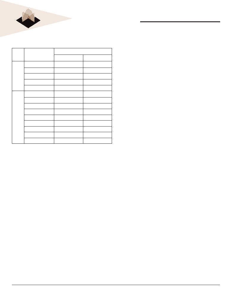
TABLE 2 – BURST DEFINITION
NOTES:
1.
For a burst length of two, A1-Ai select two-data-element block; A0 selects the
starting column within the block.
2.
For a burst length of four, A2-Ai select four-data-element block; A0-1 select the
starting column within the block.
3.
For a burst length of eight, A3-Ai select eight-data-element block; A0-2 select the
starting column within the block.
4.
Whenever a boundary of the block is reached within a given sequence above, the
following access wraps within the block.
Burst
Length
Starting Column
Address
Order of Accesses Within a Burst
Type = Sequential
Type = Interleaved
4
A1
A0
0
0-1-2-3
0
1
1-2-3-0
1-0-3-2
1
0
2-3-0-1
1
3-0-1-2
3-2-1-0
8
A2
A1
A0
0
0-1-2-3-4-5-6-7
0
1
1-2-3-0-5-6-7-4
1-0-3-2-5-4-7-6
0
1
0
2-3-0-1-6-7-4-5
0
1
3-0-1-2-7-4-5-6
3-2-1-0-7-6-5-4
1
0
4-5-6-7-0-1-2-3
1
0
1
5-6-7-4-1-2-3-0
5-4-7-6-1-0-3-2
1
0
6-7-4-5-2-3-0-1
1
7-4-5-6-3-0-1-2
7-6-5-4-3-2-1-0
OPERATING MODE
The normal operating mode is selected by issuing a
command with bit M7 set to “0,” and all other bits set to
the desired values, as shown in Figure 5. When bit M7 is
“1,” no other bits of the mode register are programmed.
Programming bit M7 to “1” places the DDR2 SDRAM into a
test mode that is only used by the manufacturer and should
not be used. No operation or functionality is guaranteed
if M7 bit is ‘1.’
DLL RESET
DLL RESET is dened by bit M8, as shown in Figure 5.
Programming bit M8 to “1” will activate the DLL RESET
function. Bit M8 is self-clearing, meaning it returns back
to a value of “0” after the DLL RESET function has been
issued.
Anytime the DLL RESET function is used, 200 clock cycles
must occur before a READ command can be issued to
allow time for the internal clock to be synchronized with the
external clock. Failing to wait for synchronization to occur
may result in a violation of the tAC or tDQSCK parameters.
WRITE RECOVERY
Write recovery (WR) time is dened by bits M9–M11, as
shown in Figure 5. The WR register is used by the DDR2
SDRAM during WRITE with auto precharge operation.
During WRITE with auto precharge operation, the DDR2
SDRAM delays the internal auto precharge operation by
WR clocks (programmed in bits M9–M11) from the last
data burst.
WR values of 2, 3, 4, 5, or 6 clocks may be used for
programming bits M9–M11. The user is required to
program the value of WR, which is calculated by dividing
tWR (in ns) by tCK (in ns) and rounding up a non integer
value to the next integer; WR [cycles] = tWR [ns] / tCK [ns].
Reserved states should not be used as unknown operation
or incompatibility with future versions may result.
POWER-DOWN MODE
Active power-down (PD) mode is dened by bit M12,
as shown in Figure 5. PD mode allows the user to
determine the active power-down mode, which determines
performance versus power savings. PD mode bit M12 does
not apply to precharge PD mode.
When bit M12 = 0, standard active PD mode or “fast-exit”
active PD mode is enabled. The tXARD parameter is used
for fast-exit active PD exit timing. The DLL is expected to
be enabled and running during this mode.
When bit M12 = 1, a lower-power active PD mode or “slow-
exit” active PD mode is enabled. The tXARD parameter is
used for slow-exit active PD exit timing. The DLL can be
enabled, but “frozen” during active PD mode since the exit-
to-READ command timing is relaxed. The power difference
expected between PD normal and PD low-power mode is
dened in the ICC table.
相關(guān)PDF資料 |
PDF描述 |
|---|---|
| W3EG72126S262AJD3SG | 128M X 72 DDR DRAM MODULE, 0.75 ns, DMA184 |
| W3EG72126S265JD3SG | 128M X 72 DDR DRAM MODULE, 0.75 ns, DMA184 |
| W3H128M72E0533SBM | DDR DRAM, PBGA208 |
| W3H128M72E2-533NBC | 128M X 72 DDR DRAM, 0.5 ns, PBGA208 |
| W7NCF01GH10CS6CG | 64M X 16 FLASH 3.3V PROM CARD, 150 ns, UUC |
相關(guān)代理商/技術(shù)參數(shù) |
參數(shù)描述 |
|---|---|
| W3H13C1048AT | 制造商:AVX 制造商全稱:AVX Corporation 功能描述:High Current Feedthry Capacitors |
| W3H13C1048AT1A | 功能描述:饋通電容器 25volt 0.1uF X7R RoHS:否 制造商:Tusonix 電容:8200 pF 容差:- 20 %, + 80 % 電壓額定值: 工作溫度范圍: 溫度系數(shù): 封裝 / 箱體: |
| W3H13C1048AT1F | 功能描述:饋通電容器 25volt 0.1uF X7R RoHS:否 制造商:Tusonix 電容:8200 pF 容差:- 20 %, + 80 % 電壓額定值: 工作溫度范圍: 溫度系數(shù): 封裝 / 箱體: |
| W3H15C1038AT | 制造商:AVX 制造商全稱:AVX Corporation 功能描述:High Current Feedthry Capacitors |
| W3H15C1038AT1A | 功能描述:饋通電容器 50volt .01uF X7R RoHS:否 制造商:Tusonix 電容:8200 pF 容差:- 20 %, + 80 % 電壓額定值: 工作溫度范圍: 溫度系數(shù): 封裝 / 箱體: |
發(fā)布緊急采購,3分鐘左右您將得到回復。