- 您現(xiàn)在的位置:買賣IC網(wǎng) > PDF目錄202172 > V58C2256804SHUD6E (PROMOS TECHNOLOGIES INC) 32M X 8 DDR DRAM, PDSO66 PDF資料下載
參數(shù)資料
| 型號: | V58C2256804SHUD6E |
| 廠商: | PROMOS TECHNOLOGIES INC |
| 元件分類: | DRAM |
| 英文描述: | 32M X 8 DDR DRAM, PDSO66 |
| 封裝: | 0.400 INCH, PLASTIC, MS-024FC, TSOP2-66 |
| 文件頁數(shù): | 21/60頁 |
| 文件大小: | 1125K |
| 代理商: | V58C2256804SHUD6E |
第1頁第2頁第3頁第4頁第5頁第6頁第7頁第8頁第9頁第10頁第11頁第12頁第13頁第14頁第15頁第16頁第17頁第18頁第19頁第20頁當(dāng)前第21頁第22頁第23頁第24頁第25頁第26頁第27頁第28頁第29頁第30頁第31頁第32頁第33頁第34頁第35頁第36頁第37頁第38頁第39頁第40頁第41頁第42頁第43頁第44頁第45頁第46頁第47頁第48頁第49頁第50頁第51頁第52頁第53頁第54頁第55頁第56頁第57頁第58頁第59頁第60頁
28
V58C2256(804/404/164)SH Rev. 1.1 July 2010
ProMOS TECHNOLOGIES
V58C2256(804/404/164)SH
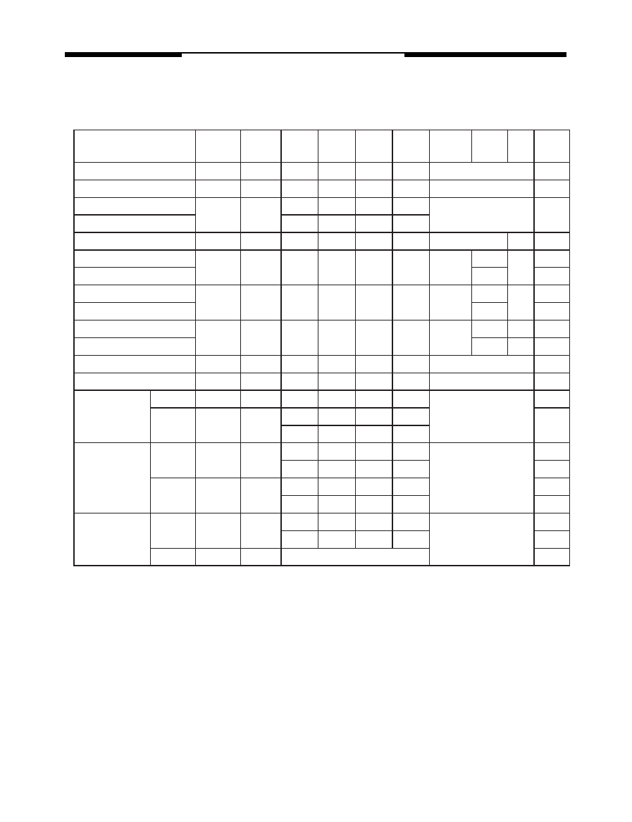
Command
CKEn-1
CKEn
CS
RAS
CAS
WE
ADDR
A10/
AP
BA
Note
H
X
LLLL
OP code
1,2
H
X
LLLL
1,2
Device Deselect
HX
H
XXX
X1
No
L
HHH
Bank Active
H
X
L
H
RA
V
1
Read
H
X
LHLH
CA
L
V
1
Read with Autoprecharge
H1,3
Write
HX
L
H
L
CA
L
V
1
Write with Autoprecharge
H1,4
Precharge All Banks
HX
L
H
L
X
HX
1,5
Precharge selected Bank
LV
1
Read Burst Stop
H
X
L
H
L
X
1
Auto
H
LLL
H
X
1
Self Refresh
Entry
H
L
LLL
H
X
1
Exit
L
H
XXX
1
LH
H
Precharge Power
Down Mode
Entry
H
L
H
XXX
X
1
LH
H
1
Exit
L
H
XXX
1
LH
H
1
Active Power
Down Mode
Entry
H
L
H
XXX
X
1
L
VVV
1
Exit
L
H
X
1
Note :
1. LDM/UDM states are Don’t Care. Refer to below Write Mask Truth Table.
2. OP Code(Operand Code) consists of A0~A11 and BA0~BA1 used for Mode Register setting during Extended MRS or MRS.
Before entering Mode Register Set mode, all banks must be in a precharge state and MRS command can be issued after tRP
period from Prechagre command.
3. If a Read with Autoprecharge command is detected by memory component in CK(n), then there will be no command presented
to activated bank until CK(n+BL/2+tRP).
4. If a Write with Autoprecharge command is detected by memory component in CK(n), then there will be no command presented
to activated bank until CK(n+BL/2+1+tDPL+tRP). Last Data-In to Prechage delay(tDPL) which is also called Write Recovery Time
(tWR) is needed to guarantee that the last data has been completely written.
5. If A10/AP is High when Precharge command being issued, BA0/BA1 are ignored and all banks are selected to be
precharged.
( H=Logic High Level, L=Logic Low Level, X=Don’t Care, V=Valid Data Input, OP Code=Operand Code, NOP=No Operation )
OP code
Refresh
Operation
Mode Register Set
Extended Mode Register Set
,6
6. This device supports concurrent auto precharge such that when a READ with auto precharge is enabled or a WRITE with auto
precharge is enabled any command to other banks is allowed, as long as that command does not interrupt the read or write
data transfer already in process. In either case, all other related limitations apply (e.g., contention between read data and write
data must be avoided).
DDR SDRAM SIMPLIFIED COMMAND TRUTH TABLE
相關(guān)PDF資料 |
PDF描述 |
|---|---|
| V58C2256804SHUI4 | 32M X 8 DDR DRAM, PDSO66 |
| V59C1512164QCF3I | 32M X 16 DDR DRAM, 0.45 ns, PBGA84 |
| V59C1G01168QBLJ-25I | DDR DRAM, PBGA84 |
| V59C1G01408QAUP25A | 256M X 4 DDR DRAM, PBGA68 |
| V59C1512164QALJ25AH | 32M X 16 DDR DRAM, PBGA92 |
相關(guān)代理商/技術(shù)參數(shù) |
參數(shù)描述 |
|---|---|
| V58C265164S | 制造商:MOSEL 制造商全稱:MOSEL 功能描述:64 Mbit DDR SDRAM 2.5 VOLT 4M X 16 |
| V58C265404S | 制造商:MOSEL 制造商全稱:MOSEL 功能描述:HIGH PERFORMANCE 2.5 VOLT 16M X 4 DDR SDRAM 4 BANKS X 4Mbit X 4 |
| V58C265804S | 制造商:MOSEL 制造商全稱:MOSEL 功能描述:HIGH PERFORMANCE 2.5 VOLT 8M X 8 DDR SDRAM 4 BANKS X 2Mbit X 8 |
| V58C3643204SAT | 制造商:MOSEL 制造商全稱:MOSEL 功能描述:HIGH PERFORMANCE 3.3 VOLT 2M X 32 DDR SDRAM 4 X 512K X 32 |
| V58C365164S | 制造商:MOSEL 制造商全稱:MOSEL 功能描述:64 Mbit DDR SDRAM 4M X 16, 3.3VOLT |
發(fā)布緊急采購,3分鐘左右您將得到回復(fù)。