- 您現(xiàn)在的位置:買(mǎi)賣IC網(wǎng) > PDF目錄300083 > V55C1256164MGLI-75H (PROMOS TECHNOLOGIES INC) SYNCHRONOUS DRAM, PDSO54 PDF資料下載
參數(shù)資料
| 型號(hào): | V55C1256164MGLI-75H |
| 廠商: | PROMOS TECHNOLOGIES INC |
| 元件分類: | DRAM |
| 英文描述: | SYNCHRONOUS DRAM, PDSO54 |
| 封裝: | 0.400 INCH, GREEN, PLASTIC, TSSOP2-54 |
| 文件頁(yè)數(shù): | 44/48頁(yè) |
| 文件大小: | 634K |
| 代理商: | V55C1256164MGLI-75H |
第1頁(yè)第2頁(yè)第3頁(yè)第4頁(yè)第5頁(yè)第6頁(yè)第7頁(yè)第8頁(yè)第9頁(yè)第10頁(yè)第11頁(yè)第12頁(yè)第13頁(yè)第14頁(yè)第15頁(yè)第16頁(yè)第17頁(yè)第18頁(yè)第19頁(yè)第20頁(yè)第21頁(yè)第22頁(yè)第23頁(yè)第24頁(yè)第25頁(yè)第26頁(yè)第27頁(yè)第28頁(yè)第29頁(yè)第30頁(yè)第31頁(yè)第32頁(yè)第33頁(yè)第34頁(yè)第35頁(yè)第36頁(yè)第37頁(yè)第38頁(yè)第39頁(yè)第40頁(yè)第41頁(yè)第42頁(yè)第43頁(yè)當(dāng)前第44頁(yè)第45頁(yè)第46頁(yè)第47頁(yè)第48頁(yè)
5
V55C1256164MG Rev. 1.0 September 2008
ProMOS TECHNOLOGIES
V55C1256164MG
Description
The V55C1256164MG is a four bank Synchronous DRAM organized as 4 banks x 4Mbit x 16. The
V55C1256164MG achieves high speed data transfer rates up to 133 MHz by employing a chip architecture
that prefetches multiple bits and then synchronizes the output data to a system clock.
All of the control, address, data input and output circuits are synchronized with the positive edge of an ex-
ternally supplied clock.
Operating the four memory banks in an interleaved fashion allows random access operation to occur at
higher rate than is possible with standard DRAMs. A sequential and gapless data rate of up to 133 MHz is
possible depending on burst length, CAS latency and speed grade of the device.
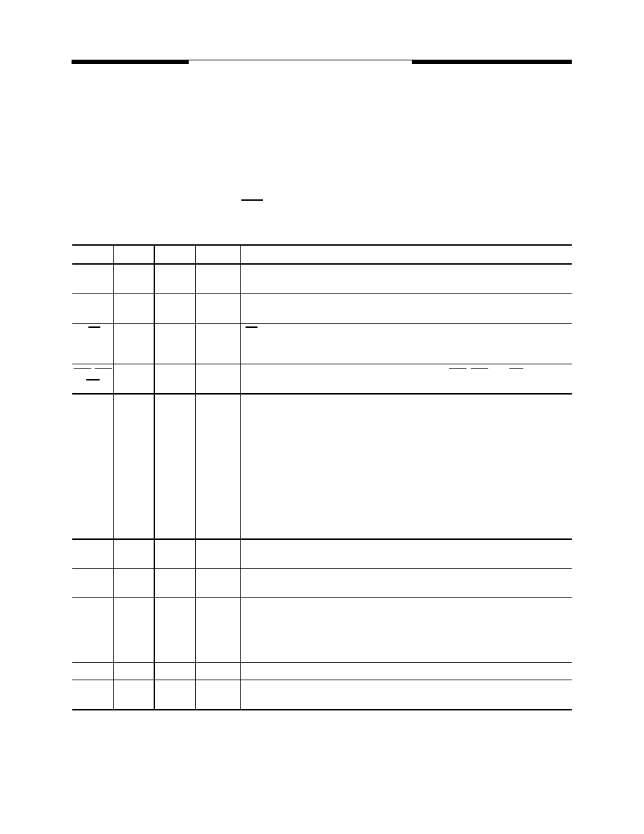
Signal Pin Description
Pin
Type
Signal
Polarity
Function
CLK
Input
Pulse
Positive
Edge
The system clock input. All of the SDRAM inputs are sampled on the rising edge of the
clock.
CKE
Input
Level
Active High Activates the CLK signal when high and deactivates the CLK signal when low, thereby
initiates either the Power Down mode or the Self Refresh mode.
CS
Input
Pulse
Active Low CS enables the command decoder when low and disables the command decoder when
high. When the command decoder is disabled, new commands are ignored but previous
operations continue.
RAS, CAS
WE
Input
Pulse
Active Low When sampled at the positive rising edge of the clock, CAS, RAS, and WE define the
command to be executed by the SDRAM.
A0 - A12
Input
Level
—
During a Bank Activate command cycle, A0-A12 defines the row address (RA0-RA12)
when sampled at the rising clock edge.
During a Read or Write command cycle, A0-An defines the column address (CA0-CAn)
when sampled at the rising clock edge.CAn depends from the SDRAM organization:
16M x 16 SDRAM CA0–CA8.
In addition to the column address, A10(=AP) is used to invoke autoprecharge operation
at the end of the burst read or write cycle. If A10 is high, autoprecharge is selected and
BA0, BA1 defines the bank to be precharged. If A10 is low, autoprecharge is disabled.
During a Precharge command cycle, A10(=AP) is used in conjunction with BA0 and BA1
to control which bank(s) to precharge. If A10 is high, all four banks will BA0 and BA1 are
used to define which bank to precharge.
BA0,
BA1
Input
Level
—
Selects which bank is to be active.
DQx
Input
Output
Level
—
Data Input/Output pins operate in the same manner as on conventional DRAMs.
LDQM
UDQM
Input
Pulse
Active High The Data Input/Output mask places the DQ buffers in a high impedance state when sam-
pled high. In Read mode, DQM has a latency of two clock cycles and controls the output
buffers like an output enable. In Write mode, DQM has a latency of zero and operates as
a word mask by allowing input data to be written if it is low but blocks the write operation
if DQM is high.
VCC, VSS
Supply
Power and ground for the input buffers and the core logic.
VCCQ
VSSQ
Supply
—
Isolated power supply and ground for the output buffers to provide improved noise
immunity.
相關(guān)PDF資料 |
PDF描述 |
|---|---|
| V55C3256164VBLG10IPC | SYNCHRONOUS DRAM, PBGA54 |
| V55C3256164VBLG8 | SYNCHRONOUS DRAM, PBGA54 |
| V55C3256164VBUC8PC | SYNCHRONOUS DRAM, PBGA54 |
| V55C3256164VBUG10E | SYNCHRONOUS DRAM, PBGA54 |
| V585ME06 | VCO, 1000 MHz - 2000 MHz |
相關(guān)代理商/技術(shù)參數(shù) |
參數(shù)描述 |
|---|---|
| V55C2128164V | 制造商:MOSEL 制造商全稱:MOSEL 功能描述:128Mbit LOW-POWER SDRAM 2.5 VOLT, TSOP II / BGA PACKAGE 8M X 16 |
| V55C2128164VB | 制造商:MOSEL 制造商全稱:MOSEL 功能描述:128Mbit LOW-POWER SDRAM 2.5 VOLT, TSOP II / BGA PACKAGE 8M X 16 |
| V55C2128164VT | 制造商:MOSEL 制造商全稱:MOSEL 功能描述:128Mbit LOW-POWER SDRAM 2.5 VOLT, TSOP II / BGA PACKAGE 8M X 16 |
| V55C2256164VB | 制造商:未知廠家 制造商全稱:未知廠家 功能描述:256Mbit MOBILE SDRAM 2.5 VOLT FBGA PACKAGE 16M X 16 |
| V55HD | 制造商:Bugera 功能描述:55 WATT GUITAR AMPLIFIER 2 CHANNEL TUBE HEAD |
發(fā)布緊急采購(gòu),3分鐘左右您將得到回復(fù)。