- 您現(xiàn)在的位置:買賣IC網(wǎng) > PDF目錄300083 > V55C1256164MGLI-75H (PROMOS TECHNOLOGIES INC) SYNCHRONOUS DRAM, PDSO54 PDF資料下載
參數(shù)資料
| 型號(hào): | V55C1256164MGLI-75H |
| 廠商: | PROMOS TECHNOLOGIES INC |
| 元件分類: | DRAM |
| 英文描述: | SYNCHRONOUS DRAM, PDSO54 |
| 封裝: | 0.400 INCH, GREEN, PLASTIC, TSSOP2-54 |
| 文件頁數(shù): | 3/48頁 |
| 文件大?。?/td> | 634K |
| 代理商: | V55C1256164MGLI-75H |
第1頁第2頁當(dāng)前第3頁第4頁第5頁第6頁第7頁第8頁第9頁第10頁第11頁第12頁第13頁第14頁第15頁第16頁第17頁第18頁第19頁第20頁第21頁第22頁第23頁第24頁第25頁第26頁第27頁第28頁第29頁第30頁第31頁第32頁第33頁第34頁第35頁第36頁第37頁第38頁第39頁第40頁第41頁第42頁第43頁第44頁第45頁第46頁第47頁第48頁
ProMOS TECHNOLOGIES
V55C1256164MG
11
V55C1256164MG Rev. 1.0 September 2008
initiated. The SDRAM automatically enters the pre-
charge operation a time delay equal to tWR (Write
recovery time) after the last data in.
Precharge Command
There is also a separate precharge command
available. When RAS and WE are low and CAS is
high at a clock timing, it triggers the precharge
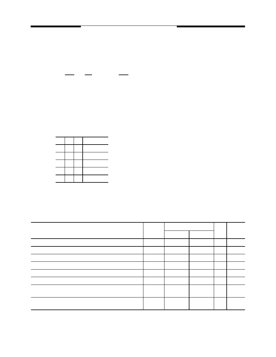
operation. Three address bits, BA0, BA1 and A10
are used to define banks as shown in the following
list. The precharge command can be imposed one
clock before the last data out for CAS latency = 2,
two clocks before the last data out for CAS latency
= 3. Writes require a time delay twr from the last
data out to apply the precharge command.
Bank Selection by Address Bits:
Burst Termination
Once a burst read or write operation has been ini-
tiated, there are several methods in which to termi-
nate the burst operation prematurely. These
methods include using another Read or Write Com-
mand to interrupt an existing burst operation, use a
Precharge Command to interrupt a burst cycle and
close the active bank, or using the Burst Stop Com-
mand to terminate the existing burst operation but
leave the bank open for future Read or Write Com-
mands to the same page of the active bank. When
interrupting a burst with another Read or Write
Command care must be taken to avoid I/O conten-
tion. The Burst Stop Command, however, has the
fewest restrictions making it the easiest method to
use when terminating a burst operation before it has
been completed. If a Burst Stop command is issued
during a burst write operation, then any residual
data from the burst write cycle will be ignored. Data
that is presented on the I/O pins before the Burst
Stop Command is registered will be written to the
memory.
A10
BA0
BA1
000
Bank 0
001
Bank 1
010
Bank 2
011
Bank 3
1
X
all Banks
Recommended Operation and Characteristics
TA = 0 to 70 °C (Commercial); -40 to 85 °C (Industrial); -40 to 105 °C (H grade); -40 to 125°C(Extended)
VSS = 0 V; VCC= 1.8 V,VCCQ = 1.8V
Note:
1.
All voltages are referenced to VSS.
2.
VIH may overshoot to VCC + 0.8 V for pulse width of < 4ns with 1.8V. VIL may undershoot to -0.8 V for pulse width < 4.0 ns with
1.8V. Pulse width measured at 50% points with amplitude measured peak to DC reference.
Parameter
Symbol
Limit Values
Unit
Notes
min.
max.
Supply voltage
VCC
1.7
1.95
V
I/O Supply Voltage
VCCQ
1.7
1.95
V
1, 2
Input high voltage (AC)
VIH
0.8xVCCQ
Vcc+0.3
V
1, 2
Input low voltage (AC)
VIL
– 0.3
0.2xVCCQ
V1, 2
Output high voltage (IOUT = – 0.1 mA)
VOH
VCCQ-0.2
–
V
Output low voltage (IOUT = 0.1 mA)
VOL
–0.2
V
Input leakage current, any input
(0 V < VIN < 3.6 V, all other inputs = 0 V)
II(L)
– 3
3
A
Output leakage current
(DQ is disabled, 0 V < VOUT < VCC)
IO(L)
– 3
3
A
Deep Power Down Mode
The Deep Power Down mode is an unique
with very low standby currents. All internal voltage
generators inside the Mobile SDRAM are stopped;
all memory data is lost in this mode. To enter the
Deep Power Down mode all banks must be prechar
ged
相關(guān)PDF資料 |
PDF描述 |
|---|---|
| V55C3256164VBLG10IPC | SYNCHRONOUS DRAM, PBGA54 |
| V55C3256164VBLG8 | SYNCHRONOUS DRAM, PBGA54 |
| V55C3256164VBUC8PC | SYNCHRONOUS DRAM, PBGA54 |
| V55C3256164VBUG10E | SYNCHRONOUS DRAM, PBGA54 |
| V585ME06 | VCO, 1000 MHz - 2000 MHz |
相關(guān)代理商/技術(shù)參數(shù) |
參數(shù)描述 |
|---|---|
| V55C2128164V | 制造商:MOSEL 制造商全稱:MOSEL 功能描述:128Mbit LOW-POWER SDRAM 2.5 VOLT, TSOP II / BGA PACKAGE 8M X 16 |
| V55C2128164VB | 制造商:MOSEL 制造商全稱:MOSEL 功能描述:128Mbit LOW-POWER SDRAM 2.5 VOLT, TSOP II / BGA PACKAGE 8M X 16 |
| V55C2128164VT | 制造商:MOSEL 制造商全稱:MOSEL 功能描述:128Mbit LOW-POWER SDRAM 2.5 VOLT, TSOP II / BGA PACKAGE 8M X 16 |
| V55C2256164VB | 制造商:未知廠家 制造商全稱:未知廠家 功能描述:256Mbit MOBILE SDRAM 2.5 VOLT FBGA PACKAGE 16M X 16 |
| V55HD | 制造商:Bugera 功能描述:55 WATT GUITAR AMPLIFIER 2 CHANNEL TUBE HEAD |
發(fā)布緊急采購,3分鐘左右您將得到回復(fù)。