- 您現(xiàn)在的位置:買(mǎi)賣(mài)IC網(wǎng) > PDF目錄361596 > UR5596 (友順科技股份有限公司) MOS IC PDF資料下載
參數(shù)資料
| 型號(hào): | UR5596 |
| 廠商: | 友順科技股份有限公司 |
| 英文描述: | MOS IC |
| 中文描述: | 馬鞍山集成電路 |
| 文件頁(yè)數(shù): | 7/11頁(yè) |
| 文件大小: | 207K |
| 代理商: | UR5596 |
UR5596
MOS IC
UNISONIC TECHNOLOGIES CO., LTD
www.unisonic.com.tw
QW-R502-045,A
7
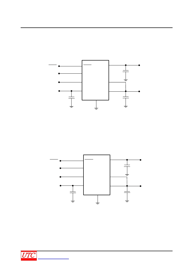
Figure 3 illustrate another application that the power rails are split when power dissipation or efficiency are
concerned. The output stage (PV
IN
) can be as lower as 1.8V, and the analog circuitry (AV
IN
) can be connected to a
higher rail such as 2.5V, 3.3V or 5V. This allows the internal power dissipation to be lowered when sourcing current
from V
TT
, but the disadvantage of this circuit is the maximum continuous current is reduced.
+
+
+
V
TT
V
DDQ
V
SENSE
V
REF
GND
SHDN
AV
IN
PV
IN
C
IN
SHDN
V
DDQ
=2.5V
AV
IN
=2.2V ~ 5.5V
C
OUT
C
REF
V
REF
=1.25V
V
TT
=1.25V
UTC UR5596
PV
IN
=1.8V
Figure 3. Lower Power Dissipation SSTL-2 Implementation
The third optional application is that PV
IN
connect to 3.3V and AV
IN
will be always limited to operation on the 3.3V
or 5V to always equal or higher than PV
IN
. This configuration has the ability to provide the maximum continuous
output current at the downside of higher thermal dissipation. The power dissipation increasing problem must be
careful to prevent the junction temperature to exceed the maximum ranting. Because of this risk it is not
recommended to supply the output stage with a voltage higher than a nominal 3.3V rail.
+
+
+
V
TT
V
DDQ
V
SENSE
V
REF
GND
SHDN
AV
IN
PV
IN
C
IN
SHDN
V
DDQ
=2.5V
AV
IN
=3.3V or 5.5V
C
OUT
C
REF
V
REF
=1.25V
V
TT
=1.25V
UTC UR5596
PV
IN
=3.3V
Figure 4. SSTL-2 Implementation with higher voltage rails
相關(guān)PDF資料 |
PDF描述 |
|---|---|
| UR5596L-S08-R | MOS IC |
| UR5596L-S08-T | MOS IC |
| UR5596-S08-R | MOS IC |
| UR5596-S08-T | MOS IC |
| UR6225-xx-AB3-C-R | 5.0 AMP POSITIVE VOLTAGE REGULATOR |
相關(guān)代理商/技術(shù)參數(shù) |
參數(shù)描述 |
|---|---|
| UR5596_07 | 制造商:UTC-IC 制造商全稱:UTC-IC 功能描述:DDR TERMINATION REGULATOR |
| UR5596_10 | 制造商:UTC-IC 制造商全稱:UTC-IC 功能描述:DDR TERMINATION REGULATOR |
| UR5596L-S08-R | 制造商:UTC-IC 制造商全稱:UTC-IC 功能描述:DDR TERMINATION REGULATOR |
| UR5596L-S08-T | 制造商:UTC-IC 制造商全稱:UTC-IC 功能描述:DDR TERMINATION REGULATOR |
| UR5596L-SH2-R | 制造商:UTC-IC 制造商全稱:UTC-IC 功能描述:DDR TERMINATION REGULATOR |
發(fā)布緊急采購(gòu),3分鐘左右您將得到回復(fù)。