- 您現在的位置:買賣IC網 > PDF目錄361594 > UPSD3334D-40U6T (意法半導體) Turbo Series Fast 8032 MCU with Programmable Logic PDF資料下載
參數資料
| 型號: | UPSD3334D-40U6T |
| 廠商: | 意法半導體 |
| 英文描述: | Turbo Series Fast 8032 MCU with Programmable Logic |
| 中文描述: | Turbo系列8032微控制器的快速可編程邏輯 |
| 文件頁數: | 43/231頁 |
| 文件大?。?/td> | 3722K |
| 代理商: | UPSD3334D-40U6T |
第1頁第2頁第3頁第4頁第5頁第6頁第7頁第8頁第9頁第10頁第11頁第12頁第13頁第14頁第15頁第16頁第17頁第18頁第19頁第20頁第21頁第22頁第23頁第24頁第25頁第26頁第27頁第28頁第29頁第30頁第31頁第32頁第33頁第34頁第35頁第36頁第37頁第38頁第39頁第40頁第41頁第42頁當前第43頁第44頁第45頁第46頁第47頁第48頁第49頁第50頁第51頁第52頁第53頁第54頁第55頁第56頁第57頁第58頁第59頁第60頁第61頁第62頁第63頁第64頁第65頁第66頁第67頁第68頁第69頁第70頁第71頁第72頁第73頁第74頁第75頁第76頁第77頁第78頁第79頁第80頁第81頁第82頁第83頁第84頁第85頁第86頁第87頁第88頁第89頁第90頁第91頁第92頁第93頁第94頁第95頁第96頁第97頁第98頁第99頁第100頁第101頁第102頁第103頁第104頁第105頁第106頁第107頁第108頁第109頁第110頁第111頁第112頁第113頁第114頁第115頁第116頁第117頁第118頁第119頁第120頁第121頁第122頁第123頁第124頁第125頁第126頁第127頁第128頁第129頁第130頁第131頁第132頁第133頁第134頁第135頁第136頁第137頁第138頁第139頁第140頁第141頁第142頁第143頁第144頁第145頁第146頁第147頁第148頁第149頁第150頁第151頁第152頁第153頁第154頁第155頁第156頁第157頁第158頁第159頁第160頁第161頁第162頁第163頁第164頁第165頁第166頁第167頁第168頁第169頁第170頁第171頁第172頁第173頁第174頁第175頁第176頁第177頁第178頁第179頁第180頁第181頁第182頁第183頁第184頁第185頁第186頁第187頁第188頁第189頁第190頁第191頁第192頁第193頁第194頁第195頁第196頁第197頁第198頁第199頁第200頁第201頁第202頁第203頁第204頁第205頁第206頁第207頁第208頁第209頁第210頁第211頁第212頁第213頁第214頁第215頁第216頁第217頁第218頁第219頁第220頁第221頁第222頁第223頁第224頁第225頁第226頁第227頁第228頁第229頁第230頁第231頁
43/231
uPSD33xx
Individual Interrupt Sources
External Interrupts Int0 and Int1.
External
terrupt inputs on pins EXTINT0 and EXTINT1
(pins 3.2 and 3.3) are either edge-triggered or lev-
el-triggered, depending on bits IT0 and IT1 in the
SFR named TCON.
When an external interrupt is generated from an
edge-triggered (falling-edge) source, the appropri-
ate flag bit (IE0 or IE1) is automatically cleared by
hardware upon entering the ISR.
When an external interrupt is generated from a
level-triggered (low-level) source, the appropriate
flag bit (IE0 or IE1) is NOT automatically cleared
by hardware.
Timer 0 and 1 Overflow Interrupt.
Timer 0 and
Timer 1 interrupts are generated by the flag bits
TF0 and TF1 when there is an overflow condition
in the respective Timer/Counter register (except
for Timer 0 in Mode 3).
Timer 2 Overflow Interrupt.
This
generated to the MCU by a logical OR of flag bits,
TF2 and EXE2. The ISR must read the flag bits to
determine the cause of the interrupt.
–
TF2 is set by an overflow of Timer 2.
–
EXE2 is generated by the falling edge of a
signal on the external pin, T2X (pin P1.1).
UART0 and UART1 Interrupt.
Each
UARTs have identical interrupt structure. For each
UART, a single interrupt is generated to the MCU
by the logical OR of the flag bits, RI (byte received)
and TI (byte transmitted).
in-
interrupt
is
of
the
The ISR must read flag bits in the SFR named
SCON0 for UART0, or SCON1 for UART1 to de-
termine the cause of the interrupt.
SPI Interrupt.
The SPI interrupt has four interrupt
sources, which are logically ORed together when
interrupting the MCU. The ISR must read the flag
bits to determine the cause of the interrupt.
A flag bit is set for: end of data transmit (TEISF);
data receive overrun (RORISF); transmit buffer
empty (TISF); or receive buffer full (RISF).
I
2
C Interrupt.
The flag bit INTR is set by a variety
of conditions occurring on the I
2
C interface: re-
ceived own slave address (ADDR flag); received
general call address (GC flag); received STOP
condition (STOP flag); or successful transmission
or reception of a data byte.The ISR must read the
flag bits to determine the cause of the interrupt.
ADC Interrupt.
The flag bit AINTF is set when an
A-to-D conversion has completed.
PCA Interrupt.
The PCA has eight interrupt
sources, which are logically ORed together when
interrupting the MCU.The ISR must read the flag
bits to determine the cause of the interrupt.
–
Each of the six TCMs can generate a "match
or capture" interrupt on flag bits OFV5..0
respectively.
–
Each of the two 16-bit counters can generate
an overflow interrupt on flag bits INTF1 and
INTF0 respectively.
Tables
17
through
Table 20., page 45
have de-
tailed bit definitions of the interrupt system SFRs.
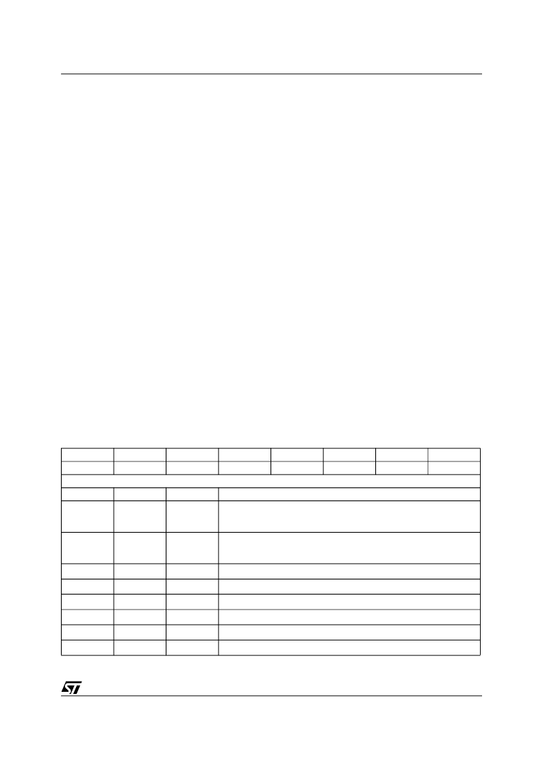
Table 17. IE: Interrupt Enable Register (SFR A8h, reset value 00h)
Bit 7
Bit 6
Bit 5
EA
–
ET2
Details
Bit
Symbol
R/W
Note: 1. 1 = Enable Interrupt, 0 = Disable Interrupt
Bit 4
ES0
Bit 3
ET1
Bit 2
EX1
Bit 1
ET0
Bit 0
EX0
Function
7
EA
R,W
Global disable bit. 0 = All interrupts are disabled. 1 = Each interrupt
source can be individually enabled or disabled by setting or clearing its
enable bit.
Do not modify this bit. It is used by the JTAG debugger for instruction
tracing. Always read the bit and write back the same bit value when
writing this SFR.
6
–
R,W
5
(1)
ET2
R,W
Enable Timer 2 Interrupt
4
(1)
ES0
R,W
Enable UART0 Interrupt
3
(1)
ET1
R,W
Enable Timer 1 Interrupt
2
(1)
EX1
R,W
Enable External Interrupt INT1
1
(1)
ET0
R,W
Enable Timer 0 Interrupt
0
(1)
EX0
R,W
Enable External Interrupt INT0
相關PDF資料 |
PDF描述 |
|---|---|
| UPSD3334DV-40T6T | Turbo Series Fast 8032 MCU with Programmable Logic |
| UPSD3334DV-40U6T | Turbo Series Fast 8032 MCU with Programmable Logic |
| UPSD3352D-40U6T | Turbo Series Fast 8032 MCU with Programmable Logic |
| UPSD3352DV-40T6T | Turbo Series Fast 8032 MCU with Programmable Logic |
| UPSD3352DV-40U6T | Turbo Series Fast 8032 MCU with Programmable Logic |
相關代理商/技術參數 |
參數描述 |
|---|---|
| UPSD3334DV40U6 | 制造商:STMicroelectronics 功能描述:MCU 8-Bit uPSD 8032 CISC 256KB Flash 3.3V 80-Pin TQFP Tray |
| UPSD3334DV-40U6 | 功能描述:8位微控制器 -MCU 256K Flash 8K SRAM RoHS:否 制造商:Silicon Labs 核心:8051 處理器系列:C8051F39x 數據總線寬度:8 bit 最大時鐘頻率:50 MHz 程序存儲器大小:16 KB 數據 RAM 大小:1 KB 片上 ADC:Yes 工作電源電壓:1.8 V to 3.6 V 工作溫度范圍:- 40 C to + 105 C 封裝 / 箱體:QFN-20 安裝風格:SMD/SMT |
| UPSD3354D-40T6 | 功能描述:8位微控制器 -MCU 8032 MCU USB RoHS:否 制造商:Silicon Labs 核心:8051 處理器系列:C8051F39x 數據總線寬度:8 bit 最大時鐘頻率:50 MHz 程序存儲器大小:16 KB 數據 RAM 大小:1 KB 片上 ADC:Yes 工作電源電壓:1.8 V to 3.6 V 工作溫度范圍:- 40 C to + 105 C 封裝 / 箱體:QFN-20 安裝風格:SMD/SMT |
| UPSD3354D-40U6 | 功能描述:8位微控制器 -MCU 8BIT Fast 8032 MCU RoHS:否 制造商:Silicon Labs 核心:8051 處理器系列:C8051F39x 數據總線寬度:8 bit 最大時鐘頻率:50 MHz 程序存儲器大小:16 KB 數據 RAM 大小:1 KB 片上 ADC:Yes 工作電源電壓:1.8 V to 3.6 V 工作溫度范圍:- 40 C to + 105 C 封裝 / 箱體:QFN-20 安裝風格:SMD/SMT |
| UPSD3354DV-40T6 | 功能描述:8位微控制器 -MCU 8032 MCU USB RoHS:否 制造商:Silicon Labs 核心:8051 處理器系列:C8051F39x 數據總線寬度:8 bit 最大時鐘頻率:50 MHz 程序存儲器大小:16 KB 數據 RAM 大小:1 KB 片上 ADC:Yes 工作電源電壓:1.8 V to 3.6 V 工作溫度范圍:- 40 C to + 105 C 封裝 / 箱體:QFN-20 安裝風格:SMD/SMT |
發(fā)布緊急采購,3分鐘左右您將得到回復。