- 您現(xiàn)在的位置:買賣IC網(wǎng) > PDF目錄373745 > TSS463A-TERZ (Atmel Corp.) VAN Data Link Controller with Serial Interface PDF資料下載
參數(shù)資料
| 型號: | TSS463A-TERZ |
| 廠商: | Atmel Corp. |
| 英文描述: | VAN Data Link Controller with Serial Interface |
| 中文描述: | 凡數(shù)據(jù)與串行接口鏈路控制器 |
| 文件頁數(shù): | 9/60頁 |
| 文件大小: | 816K |
| 代理商: | TSS463A-TERZ |
第1頁第2頁第3頁第4頁第5頁第6頁第7頁第8頁當前第9頁第10頁第11頁第12頁第13頁第14頁第15頁第16頁第17頁第18頁第19頁第20頁第21頁第22頁第23頁第24頁第25頁第26頁第27頁第28頁第29頁第30頁第31頁第32頁第33頁第34頁第35頁第36頁第37頁第38頁第39頁第40頁第41頁第42頁第43頁第44頁第45頁第46頁第47頁第48頁第49頁第50頁第51頁第52頁第53頁第54頁第55頁第56頁第57頁第58頁第59頁第60頁
9
TSS463-AA
4205B–AUTO–12/04
The master device provides the serial clock on the TxD pin and is still connected to
SCLK pin of the slave device.
Then, the RxD replaces the MOSI and MISO pins and is a bi-directional pin. To achieve
a correct communication, the user should add a few gates to connect the master RxD
pin to the MOSI-MISO slave pins.
Figure 5 proposes two 3-state buffers controlled by the master through a general pur-
pose I/O pin.
It is obvious that, in this Intel SPI mode, the master cannot monitor the "0xAA and 0x55"
synchronization bytes while sending the address and control bytes. It is the only excep-
tion in this mode compared with the Motorola SPI mode.
SCI Mode
The SCI mode is the third type of interface. The TSS463AA enters this mode if the Ini-
tialization Sequence contains (first two bytes received) "0x00, 0xFF".
The SCI is compatible with a 9-bits SCI protocol. The interface is implemented for slave-
mode only (the TSS463AA cannot generate SCI frames by itself).
The SCI interface allows an interconnection of several CPUs and peripherals on the
same printed circuit board.
The SCI mode interface consists of 4 pins: separate wires are required for data and
clock, so the clock is not included in the data stream as shown in Figure 6. One pin is
needed for the serial clock (SCLK), two pins for data exchange MOSI and MISO and
one pin for Slave Select SS.
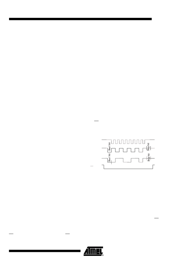
Figure 6.
SCI Data Stream
SCLK: Serial Clock
The master device provides the serial clock for the slave devices. Data is transferred
synchronously with this clock in both directions. The master and the slave devices
exchange a data byte during a
nine
clock pulses sequence. However, the TSS463AA
will only monitor 8 bits on its MOSI line and send 9 bits on its MISO line.
MOSI: Master Out Slave In
The MOSI pin is the master device data output (CPU) and the slave device data input
(TSS463AA). Data is transferred serially from the master to the slave on this line;
least
significant bit (LSB) first,
most
significant bit (MSB) last. The TSS463AA will only moni-
tor 8 bits starting from the LSB to MSB-1.
MISO: Master In Slave Out
The MISO pin is configured as the slave device data output (TSS463AA) and as master
device data input (CPU). When the slave device is not selected (SS = 1), this pin is in
high impedance state. The value of the MSB (9
th
bit) sent on the MISO pin will always be
"1" and should not be used by the master.
SS: Slave Select
The SS pin is the slave chip select. It is low active. A low state on the Slave Select input
allows the TSS463AA to accept data on the MOSI pin and send data on the MISO pin.
MOSI
MISO
0x55
SS
SCLK
SCI 9 Pulses
0x66
相關PDF資料 |
PDF描述 |
|---|---|
| TSS463C | VAN Data Link Controller with Serial Interface |
| TSS4B02G | Single Phase 4.0 Amps. Glass Passivated Super Fast Bridge Rectifiers |
| TSS4B03G | Single Phase 4.0 Amps. Glass Passivated Super Fast Bridge Rectifiers |
| TSS4B01G | Single Phase 4.0 Amps. Glass Passivated Super Fast Bridge Rectifiers |
| TSS5G45S | TOSHIBA SOLID STATE AC RELAY |
相關代理商/技術參數(shù) |
參數(shù)描述 |
|---|---|
| TSS463B | 制造商:ATMEL 制造商全稱:ATMEL Corporation 功能描述:Serial VAN Data Link Controller |
| TSS463B_03 | 制造商:ATMEL 制造商全稱:ATMEL Corporation 功能描述:Serial VAN Data Link Controller |
| TSS463B_04 | 制造商:ATMEL 制造商全稱:ATMEL Corporation 功能描述:VAN Data Link Controller with Serial Interface |
| TSS463B-TERA | 制造商:Temic 功能描述:LAN Node Controller, 16 Pin, SOP |
| TSS463B-TERA-9 | 制造商:ATMEL 制造商全稱:ATMEL Corporation 功能描述:VAN Data Link Controller with Serial Interface |
發(fā)布緊急采購,3分鐘左右您將得到回復。