- 您現(xiàn)在的位置:買賣IC網(wǎng) > PDF目錄368671 > TMS320C241 16-Bit Digital Signal Processor PDF資料下載
參數(shù)資料
| 型號: | TMS320C241 |
| 元件分類: | 數(shù)字信號處理 |
| 英文描述: | 16-Bit Digital Signal Processor |
| 中文描述: | 16位數(shù)字信號處理器 |
| 文件頁數(shù): | 24/66頁 |
| 文件大小: | 803K |
| 代理商: | TMS320C241 |
第1頁第2頁第3頁第4頁第5頁第6頁第7頁第8頁第9頁第10頁第11頁第12頁第13頁第14頁第15頁第16頁第17頁第18頁第19頁第20頁第21頁第22頁第23頁當前第24頁第25頁第26頁第27頁第28頁第29頁第30頁第31頁第32頁第33頁第34頁第35頁第36頁第37頁第38頁第39頁第40頁第41頁第42頁第43頁第44頁第45頁第46頁第47頁第48頁第49頁第50頁第51頁第52頁第53頁第54頁第55頁第56頁第57頁第58頁第59頁第60頁第61頁第62頁第63頁第64頁第65頁第66頁
TMS320C242
DSP CONTROLLER
SPRS063B – DECEMBER 1997 – REVISED DECEMBER 1999
24
POST OFFICE BOX 1443
HOUSTON, TEXAS 77251–1443
clock domains (continued)
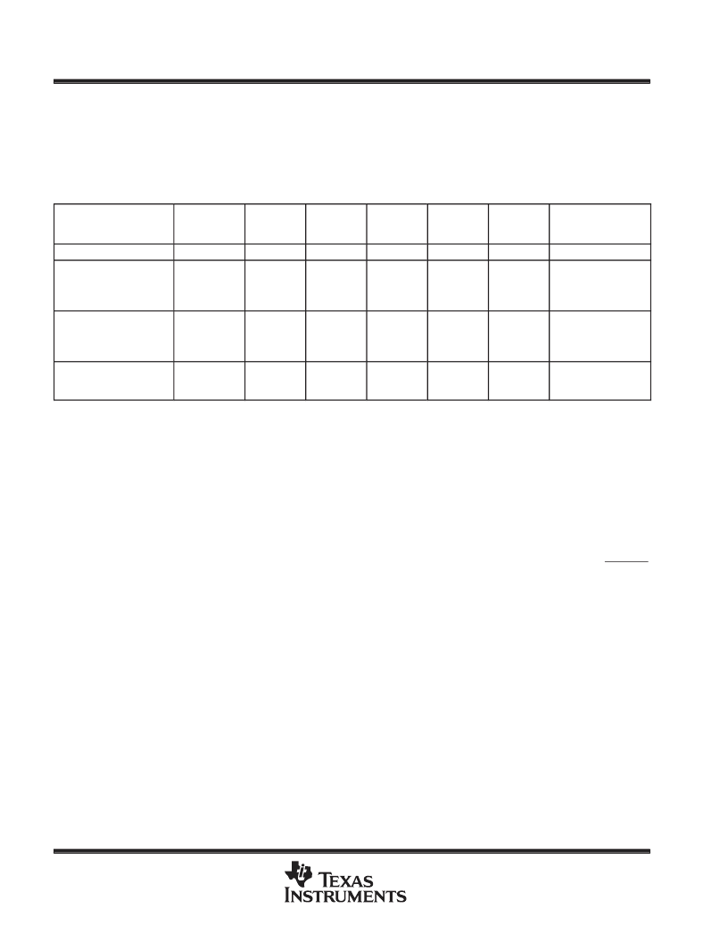
Two control bits, LPM(1) and LPM(0), specify which of the three possible low-power modes is entered when
the IDLE instruction is executed (see Table 7). These bits are located in the System Control and Status Register
(SCSR) described in the TMS320F243,F241,C242 DSP Controllers System and Peripherals User’s Guide
Volume 2 (literature number SPRU276).
Table 7. Low-Power Modes Summary
LOW-POWER MODE
LPMx BITS
SCSR[13:12]
CPU
CLOCK
DOMAIN
SYSTEM
CLOCK
DOMAIN
WDCLK
STATUS
PLL
STATUS
OSC
STATUS
EXIT
CONDITION
CPU running normally
XX
On
On
On
On
On
—
IDLE1 – (LPM0)
00
Off
On
On
On
On
Peripheral Interrupt,
External Interrupt,
Reset
IDLE2 – (LPM1)
01
Off
Off
On
On
On
Wakeup Interrupts,
External Interrupt,
Reset
HALT – (LPM2)
{PLL/OSC power down}
1X
Off
Off
Off
Off
Off
Reset Only
wakeup from low-power modes
reset
A reset (from any source) causes the device to exit any of the IDLE modes. If the device is halted, the reset will
first start the oscillator, and there can be a delay while the oscillator powers up before clocks are generated to
initiate the CPU reset sequence.
external interrupts
The external interrupts, XINTx, can cause the device to exit any of the low-power modes, except HALT. If the
device is in IDLE2 mode, the synchronous logic connected to the external interrupt pins is bypassed with
combinatorial logic which recognizes the interrupt on the pin, starts the clocks, and then allows the clocked logic
to generate an interrupt request to the PIE controller. Note that in Table 7, external interrupts include PDPINT.
A
相關(guān)PDF資料 |
PDF描述 |
|---|---|
| TMS320C242FNS | 16-Bit Digital Signal Processor |
| TMS320C242PGA | 16-Bit Digital Signal Processor |
| TMS320C242PGS | 16-Bit Digital Signal Processor |
| TMS320C30GEL | 32-Bit Digital Signal Processor |
| SM320C25FJM | 16-Bit Digital Signal Processor |
相關(guān)代理商/技術(shù)參數(shù) |
參數(shù)描述 |
|---|---|
| TMS320C241FNS | 制造商:未知廠家 制造商全稱:未知廠家 功能描述:16-Bit Digital Signal Processor |
| TMS320C241PGS | 制造商:未知廠家 制造商全稱:未知廠家 功能描述:16-Bit Digital Signal Processor |
| TMS320C242 | 制造商:TI 制造商全稱:Texas Instruments 功能描述:DSP CONTROLLER |
| TMS320C242FN | 制造商:TI 制造商全稱:Texas Instruments 功能描述:DSP CONTROLLER |
| TMS320C242FNA | 制造商:未知廠家 制造商全稱:未知廠家 功能描述:16-Bit Digital Signal Processor |
發(fā)布緊急采購,3分鐘左右您將得到回復。