- 您現(xiàn)在的位置:買賣IC網(wǎng) > PDF目錄368672 > TMS320C240PQL 16-Bit Microcontroller PDF資料下載
參數(shù)資料
| 型號(hào): | TMS320C240PQL |
| 英文描述: | 16-Bit Microcontroller |
| 中文描述: | 16位微控制器 |
| 文件頁數(shù): | 89/105頁 |
| 文件大小: | 1481K |
| 代理商: | TMS320C240PQL |
第1頁第2頁第3頁第4頁第5頁第6頁第7頁第8頁第9頁第10頁第11頁第12頁第13頁第14頁第15頁第16頁第17頁第18頁第19頁第20頁第21頁第22頁第23頁第24頁第25頁第26頁第27頁第28頁第29頁第30頁第31頁第32頁第33頁第34頁第35頁第36頁第37頁第38頁第39頁第40頁第41頁第42頁第43頁第44頁第45頁第46頁第47頁第48頁第49頁第50頁第51頁第52頁第53頁第54頁第55頁第56頁第57頁第58頁第59頁第60頁第61頁第62頁第63頁第64頁第65頁第66頁第67頁第68頁第69頁第70頁第71頁第72頁第73頁第74頁第75頁第76頁第77頁第78頁第79頁第80頁第81頁第82頁第83頁第84頁第85頁第86頁第87頁第88頁當(dāng)前第89頁第90頁第91頁第92頁第93頁第94頁第95頁第96頁第97頁第98頁第99頁第100頁第101頁第102頁第103頁第104頁第105頁
TMS320C240, TMS320F240
DSP CONTROLLERS
SPRS042D – OCTOBER 1996 – REVISED NOVEMBER 1998
89
POST OFFICE BOX 1443
HOUSTON, TEXAS 77251–1443
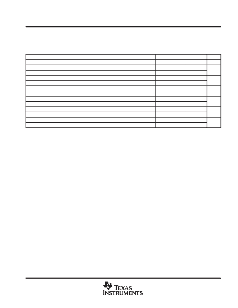
SPI SLAVE MODE TIMING PARAMETERS
Slave mode timing information is listed in the following tables.
SPI slave mode external timing parameters (clock phase = 0)
(see Figure 45)
MIN
MAX
UNIT
tc(SPC)S
tw(SPCH)S§
tw(SPCL)S§
tw(SPCL)S§
tw(SPCH)S§
td(SPCH-SOMI)S§
td(SPCL-SOMI)S§
tv(SPCL-SOMI)S§
tv(SPCH-SOMI)S§
tsu(SIMO-SPCL)S§
tsu(SIMO-SPCH)S§
tv(SPCL-SIMO)S§
tv(SPCH-SIMO)S§
The MASTER/SLAVE bit (SPICTL.2) is cleared and the CLOCK PHASE bit (SPICTL.3) is cleared.
tc = system clock cycle time = 1/SYSCLK = tc(SYS)
§The active edge of the SPICLK signal referenced is controlled by the CLOCK POLARITY bit (SPICCR.6).
Cycle time, SPICLK
8tc
ns
Pulse duration, SPICLK high (clock polarity = 0)
0.5tc(SPC)S–70
0.5tc(SPC)S–70
0.5tc(SPC)S–70
0.5tc(SPC)S–70
0.375tc(SPC)S–70
0.375tc(SPC)S–70
0.75tc(SPC)S
0.75tc(SPC)S
0
0.5tc(SPC)S
0.5tc(SPC)S
0.5tc(SPC)S
0.5tc(SPC)S
ns
Pulse duration, SPICLK low (clock polarity = 1)
Pulse duration, SPICLK low (clock polarity = 0)
ns
Pulse duration, SPICLK high (clock polarity = 1)
Delay time, SPICLK high (clock polarity = 0) to SPISOMI valid
ns
Delay time, SPICLK low (clock polarity = 1) to SPISOMI valid
Valid time, SPISOMI data valid after SPICLK low (clock polarity =0)
ns
Valid time, SPISOMI data valid after SPICLK high (clock polarity =1)
Setup time, SPISIMO before SPICLK low (clock polarity = 0)
ns
Setup time, SPISIMO before SPICLK high (clock polarity = 1)
0
Valid time, SPISIMO data valid after SPICLK low (clock polarity = 0)
Valid time, SPISIMO data valid after SPICLK high (clock polarity = 1)
0.5tc(SPC)S
0.5tc(SPC)S
ns
相關(guān)PDF資料 |
PDF描述 |
|---|---|
| TMS320C240PQQ | 16-Bit Microcontroller |
| TMS320F240PQL | 16-Bit Microcontroller |
| TMS320F240PQQ | 16-Bit Microcontroller |
| TMS320F240PQS | 16-Bit Microcontroller |
| TMS320LC31-40 | Digital Signal Processor |
相關(guān)代理商/技術(shù)參數(shù) |
參數(shù)描述 |
|---|---|
| TMS320C240PQQ | 制造商:未知廠家 制造商全稱:未知廠家 功能描述:16-Bit Microcontroller |
| TMS320C241 | 制造商:未知廠家 制造商全稱:未知廠家 功能描述:16-Bit Digital Signal Processor |
| TMS320C241FNS | 制造商:未知廠家 制造商全稱:未知廠家 功能描述:16-Bit Digital Signal Processor |
| TMS320C241PGS | 制造商:未知廠家 制造商全稱:未知廠家 功能描述:16-Bit Digital Signal Processor |
| TMS320C242 | 制造商:TI 制造商全稱:Texas Instruments 功能描述:DSP CONTROLLER |
發(fā)布緊急采購,3分鐘左右您將得到回復(fù)。