- 您現(xiàn)在的位置:買賣IC網(wǎng) > PDF目錄98149 > SX28AC/SSU 2 CHANNEL(S), I2C BUS CONTROLLER, PDSO28 PDF資料下載
參數(shù)資料
| 型號: | SX28AC/SSU |
| 元件分類: | 微控制器/微處理器 |
| 英文描述: | 2 CHANNEL(S), I2C BUS CONTROLLER, PDSO28 |
| 封裝: | GREEN, PLASTIC, SSOP-28 |
| 文件頁數(shù): | 46/48頁 |
| 文件大小: | 772K |
| 代理商: | SX28AC/SSU |
第1頁第2頁第3頁第4頁第5頁第6頁第7頁第8頁第9頁第10頁第11頁第12頁第13頁第14頁第15頁第16頁第17頁第18頁第19頁第20頁第21頁第22頁第23頁第24頁第25頁第26頁第27頁第28頁第29頁第30頁第31頁第32頁第33頁第34頁第35頁第36頁第37頁第38頁第39頁第40頁第41頁第42頁第43頁第44頁第45頁當(dāng)前第46頁第47頁第48頁
2005 Ubicom, Inc. All rights reserved.
- 7 -
www.ubicom.com
SX20AC/SX28AC
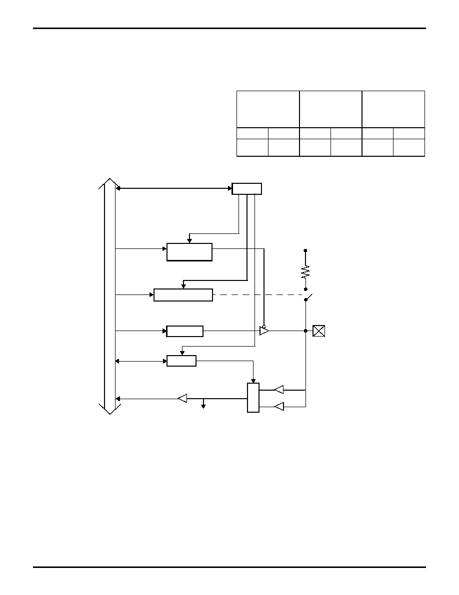
3.0 PORT DESCRIPTIONS
The device contains a 4-bit I/O port (Port A) and two 8-bit
I/O ports (Port B, Port C). Port A provides symmetrical
drive capability. Each port has four associated 8-bit regis-
ters (Direction, Data, TTL/CMOS Select, and Pull-Up
Enable) to configure each port pin as Hi-Z input or output,
to select TTL or CMOS voltage levels, and to enable/dis-
able the weak pull-up resistor. The upper four bits of the
registers associated with Port A are not used. The least
significant bit of the registers corresponds to the least
significant port pin. To access these registers, an appro-
priate value must be written into the MODE register.
Upon power-up, all bits in these registers are initialized to
“1” (except that the Data registers are undefined on
power-up).
The associated registers allow for each port bit to be indi-
vidually configured under software control as shown
below:
Port B and Port C have additional associated registers
3.1 Reading and Writing the Ports
The three ports are memory-mapped into the data mem-
ory address space. To the CPU, the three ports are avail-
able as the RA, RB, and RC file registers at data memory
addresses 05h, 06h, and 07h, respectively.
Writing to a port data register sets the voltage levels of
the corresponding port pins that have been configured to
operate as outputs. Reading from a port data register
reads the voltage levels of the corresponding port pins
that have been configured as inputs.
Table 3-1. Port Configuration
Direction
Registers:
RA, RB, RC
TTL/CMOS
Select Registers:
LVL_A, LVL_B,
LVL_C
Pullup Enable
Registers:
PLP_A, PLP_B,
PLP_C
01010
1
Output
Hi-Z
Input
CMOS
TTL
Enable
Disable
Figure 3-1. Port A Configuration
MODE
RA
RA Data
LVL_A
0 = Output
1 = Hi-Z Input
WR
0 = CMOS
1 = TTL
RD
TTL Buffer
CMOS Buffer
Vdd
Pullup
Port A PIN
Internal
Dat
aBus
M
U
X
Mode
=
0
F
Mode
=
0
E
Mode
=
0
D
WR
Direction
PLP_A
0 = Pullup Enable
1 = Pullup Disable
Port A INPUT
WR
相關(guān)PDF資料 |
PDF描述 |
|---|---|
| SY100EP11UZITR | 100E SERIES, LOW SKEW CLOCK DRIVER, 2 TRUE OUTPUT(S), 0 INVERTED OUTPUT(S), PDSO8 |
| SY100EP195VTCTR | ACTIVE DELAY LINE, COMPLEMENTARY OUTPUT, PQFP32 |
| SY100EP195VTG | ACTIVE DELAY LINE, COMPLEMENTARY OUTPUT, PQFP32 |
| SY100EP196VTCTR | ACTIVE DELAY LINE, COMPLEMENTARY OUTPUT, PQFP32 |
| SY100EP196VTC | ACTIVE DELAY LINE, COMPLEMENTARY OUTPUT, PQFP32 |
相關(guān)代理商/技術(shù)參數(shù) |
參數(shù)描述 |
|---|---|
| SX28AD100-I/DP | 制造商:未知廠家 制造商全稱:未知廠家 功能描述:Configurable Communications Controllers with EE/Flash Program Memory, In-System Programming Capability and On-Chip Debug |
| SX28AD100-I/PQ | 制造商:未知廠家 制造商全稱:未知廠家 功能描述:Configurable Communications Controllers with EE/Flash Program Memory, In-System Programming Capability and On-Chip Debug |
| SX28AD100-I/SO | 制造商:未知廠家 制造商全稱:未知廠家 功能描述:Configurable Communications Controllers with EE/Flash Program Memory, In-System Programming Capability and On-Chip Debug |
| SX28AD100-I/SS | 制造商:未知廠家 制造商全稱:未知廠家 功能描述:Configurable Communications Controllers with EE/Flash Program Memory, In-System Programming Capability and On-Chip Debug |
| SX28AD100-I/TQ | 制造商:未知廠家 制造商全稱:未知廠家 功能描述:Configurable Communications Controllers with EE/Flash Program Memory, In-System Programming Capability and On-Chip Debug |
發(fā)布緊急采購,3分鐘左右您將得到回復(fù)。