- 您現(xiàn)在的位置:買賣IC網(wǎng) > PDF目錄98145 > ST72F651AR6T1 (STMICROELECTRONICS) 8-BIT, FLASH, MICROCONTROLLER, PQFP64 PDF資料下載
參數(shù)資料
| 型號: | ST72F651AR6T1 |
| 廠商: | STMICROELECTRONICS |
| 元件分類: | 微控制器/微處理器 |
| 英文描述: | 8-BIT, FLASH, MICROCONTROLLER, PQFP64 |
| 封裝: | 10 X 10 MM, ROHS COMPLIANT, TQFP-64 |
| 文件頁數(shù): | 146/161頁 |
| 文件大小: | 2656K |
| 代理商: | ST72F651AR6T1 |
第1頁第2頁第3頁第4頁第5頁第6頁第7頁第8頁第9頁第10頁第11頁第12頁第13頁第14頁第15頁第16頁第17頁第18頁第19頁第20頁第21頁第22頁第23頁第24頁第25頁第26頁第27頁第28頁第29頁第30頁第31頁第32頁第33頁第34頁第35頁第36頁第37頁第38頁第39頁第40頁第41頁第42頁第43頁第44頁第45頁第46頁第47頁第48頁第49頁第50頁第51頁第52頁第53頁第54頁第55頁第56頁第57頁第58頁第59頁第60頁第61頁第62頁第63頁第64頁第65頁第66頁第67頁第68頁第69頁第70頁第71頁第72頁第73頁第74頁第75頁第76頁第77頁第78頁第79頁第80頁第81頁第82頁第83頁第84頁第85頁第86頁第87頁第88頁第89頁第90頁第91頁第92頁第93頁第94頁第95頁第96頁第97頁第98頁第99頁第100頁第101頁第102頁第103頁第104頁第105頁第106頁第107頁第108頁第109頁第110頁第111頁第112頁第113頁第114頁第115頁第116頁第117頁第118頁第119頁第120頁第121頁第122頁第123頁第124頁第125頁第126頁第127頁第128頁第129頁第130頁第131頁第132頁第133頁第134頁第135頁第136頁第137頁第138頁第139頁第140頁第141頁第142頁第143頁第144頁第145頁當前第146頁第147頁第148頁第149頁第150頁第151頁第152頁第153頁第154頁第155頁第156頁第157頁第158頁第159頁第160頁第161頁
ST72651AR6
85/161
Doc ID 7215 Rev 4
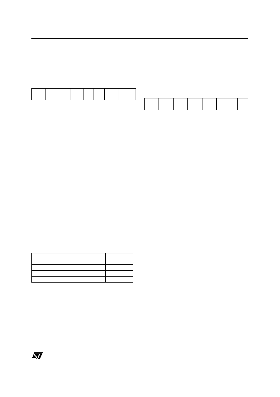
16-BIT TIMER (Cont’d)
CONTROL REGISTER 2 (TCR2)
Read/Write
Reset Value: 0000 0000 (00h)
Bit 7 = OC1E Output Compare 1 Pin Enable.
This bit is used only to output the signal from the
timer on the OCMP1 pin (OLV1 in Output Com-
pare mode). Whatever the value of the OC1E bit,
the internal Output Compare 1 function of the timer
remains active.
0: OCMP1 pin alternate function disabled (I/O pin
free for general-purpose I/O).
1: OCMP1 pin alternate function enabled.
Bit 6 = OC2E Output Compare 2 Pin Enable.
This bit is used only to output the signal from the
timer on the OCMP2 pin (OLV2 in Output Com-
pare mode). Whatever the value of the OC2E bit,
the internal Output Compare 2 function of the timer
remains active.
0: OCMP2 pin alternate function disabled (I/O pin
free for general-purpose I/O).
1: OCMP2 pin alternate function enabled.
Bits 5:4 = Reserved, forced by hardware to 0.
Bits 3:2 = CC[1:0] Clock Control.
The timer clock mode depends on these bits:
Table 27. Clock Control Bits
Bits 1:0 = Reserved, forced by hardware to 0.
STATUS REGISTER (TSR)
Read Only
Reset Value: 0000 0000 (00h)
The three least significant bits are not used.
Bit 7 = Reserved, forced by hardware to 0.
Bit 6 = OCF1 Output Compare Flag 1.
0: No match (reset value).
1: The content of the free running counter has
matched the content of the OC1R register. To
clear this bit, first read the SR register, then read
or write the low byte of the OC1R (OC1LR) reg-
ister.
Bit 5 = TOF Timer Overflow Flag.
0: No timer overflow (reset value).
1: The free running counter rolled over from FFFFh
to 0000h. To clear this bit, first read the SR reg-
ister, then read or write the low byte of the CR
(CLR) register.
Note: Reading or writing the ACLR register does
not clear TOF.
Bit 4 = Reserved, forced by hardware to 0.
Bit 3 = OCF2 Output Compare Flag 2.
0: No match (reset value).
1: The content of the free running counter has
matched the content of the OC2R register. To
clear this bit, first read the SR register, then read
or write the low byte of the OC2R (OC2LR) reg-
ister.
Bits 2:0 = Reserved, forced by hardware to 0.
70
OC1E OC2E
0
CC1 CC0
0
Timer Clock
CC1
CC0
fCPU / 4
0
fCPU / 2
0
1
fCPU / 8
1
0
Reserved
1
70
0OCF1
TOF
0OCF2
0
相關(guān)PDF資料 |
PDF描述 |
|---|---|
| ST72P60E2M1 | 8-BIT, MROM, 8 MHz, MICROCONTROLLER, PDSO24 |
| ST7260E2M1/XXX | 8-BIT, MROM, 8 MHz, MICROCONTROLLER, PDSO24 |
| ST72T141K2M6XXX | 8-BIT, OTPROM, 8 MHz, MICROCONTROLLER, PDSO34 |
| ST72T141K2M3XXX | 8-BIT, OTPROM, 8 MHz, MICROCONTROLLER, PDSO34 |
| ST72T141K2MARE | 8-BIT, OTPROM, 8 MHz, MICROCONTROLLER, PDSO34 |
相關(guān)代理商/技術(shù)參數(shù) |
參數(shù)描述 |
|---|---|
| ST72F651AR6T1E | 功能描述:8位微控制器 -MCU Flash 32K USB/DTC/I2 RoHS:否 制造商:Silicon Labs 核心:8051 處理器系列:C8051F39x 數(shù)據(jù)總線寬度:8 bit 最大時鐘頻率:50 MHz 程序存儲器大小:16 KB 數(shù)據(jù) RAM 大小:1 KB 片上 ADC:Yes 工作電源電壓:1.8 V to 3.6 V 工作溫度范圍:- 40 C to + 105 C 封裝 / 箱體:QFN-20 安裝風格:SMD/SMT |
| ST72P262M6/OZXTR | 制造商:STMicroelectronics 功能描述:ST72P262M6/OZXTR |
| ST72P324TA/OBZTR | 制造商:STMicroelectronics 功能描述: |
| ST72P324TA/OHXTR | 制造商:STMicroelectronics 功能描述: |
| ST72P4T128M-A05AU | 制造商:STEC Inc 功能描述:1GB,ECC,REG,DDR2-400,UNLEAD - Bulk |
發(fā)布緊急采購,3分鐘左右您將得到回復(fù)。