- 您現(xiàn)在的位置:買賣IC網(wǎng) > PDF目錄231009 > S71PL032J80BAW074 (SPANSION LLC) SPECIALTY MEMORY CIRCUIT, PBGA56 PDF資料下載
參數(shù)資料
| 型號: | S71PL032J80BAW074 |
| 廠商: | SPANSION LLC |
| 元件分類: | 存儲器 |
| 英文描述: | SPECIALTY MEMORY CIRCUIT, PBGA56 |
| 封裝: | 7 X 9 MM, 1.20 MM HEIGHT, FBGA-56 |
| 文件頁數(shù): | 32/188頁 |
| 文件大小: | 5078K |
| 代理商: | S71PL032J80BAW074 |
第1頁第2頁第3頁第4頁第5頁第6頁第7頁第8頁第9頁第10頁第11頁第12頁第13頁第14頁第15頁第16頁第17頁第18頁第19頁第20頁第21頁第22頁第23頁第24頁第25頁第26頁第27頁第28頁第29頁第30頁第31頁當前第32頁第33頁第34頁第35頁第36頁第37頁第38頁第39頁第40頁第41頁第42頁第43頁第44頁第45頁第46頁第47頁第48頁第49頁第50頁第51頁第52頁第53頁第54頁第55頁第56頁第57頁第58頁第59頁第60頁第61頁第62頁第63頁第64頁第65頁第66頁第67頁第68頁第69頁第70頁第71頁第72頁第73頁第74頁第75頁第76頁第77頁第78頁第79頁第80頁第81頁第82頁第83頁第84頁第85頁第86頁第87頁第88頁第89頁第90頁第91頁第92頁第93頁第94頁第95頁第96頁第97頁第98頁第99頁第100頁第101頁第102頁第103頁第104頁第105頁第106頁第107頁第108頁第109頁第110頁第111頁第112頁第113頁第114頁第115頁第116頁第117頁第118頁第119頁第120頁第121頁第122頁第123頁第124頁第125頁第126頁第127頁第128頁第129頁第130頁第131頁第132頁第133頁第134頁第135頁第136頁第137頁第138頁第139頁第140頁第141頁第142頁第143頁第144頁第145頁第146頁第147頁第148頁第149頁第150頁第151頁第152頁第153頁第154頁第155頁第156頁第157頁第158頁第159頁第160頁第161頁第162頁第163頁第164頁第165頁第166頁第167頁第168頁第169頁第170頁第171頁第172頁第173頁第174頁第175頁第176頁第177頁第178頁第179頁第180頁第181頁第182頁第183頁第184頁第185頁第186頁第187頁第188頁
128
pSRAM Type 7
pSRAM_Type07_13_A0 May 4, 2004
Prelimin ary
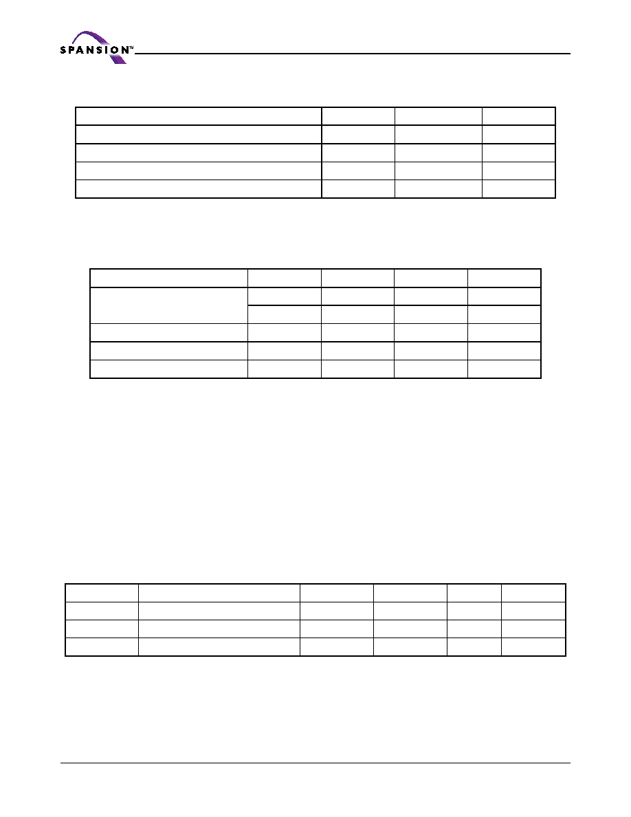
Absolute Maximum Ratings
WARNING: Semiconductor devices can be permanently damaged by application of stress (voltage, current, temperature,
etc.) in excess of absolute maximum ratings. Do not exceed these ratings.
Recommended Operating Conditions (See Warning Below)
Notes:
1. Maximum DC voltage on input and I/O pins are VDD+0.2V. During voltage transitions, inputs may positive overshoot to
VDD+1.0V for periods of up to 5 ns.
2. Minimum DC voltage on input or I/O pins are -0.3V. During voltage transitions, inputs may negative overshoot VSS to -1.0V
for periods of up to 5ns.
WARNING: Recommended operating conditions are normal operating ranges for the semiconductor device. All the de-
vice’s electrical characteristics are warranted when operated within these ranges.
Always use semiconductor devices within the recommended operating conditions. Operation outside these ranges may
adversely affect reliability and could result in device failure.
No warranty is made with respect to uses, operating conditions, or combinations not represented on the data sheet.
Users considering application outside the listed conditions are advised to contact their FUJITSU representative before-
hand.
Package Capacitance
Test conditions: TA = 25°C, f = 1.0 MHz
Item
Symbol
Value
Unit
Voltage of VDD Supply Relative to VSS
VDD
-0.5 to +3.6
V
Voltage at Any Pin Relative to VSS
VIN, VOUT
-0.5 to +3.6
V
Short Circuit Output Current
IOUT
±50
mA
Storage temperature
TSTG
-55 to +125
°C
Parameter
Symbol
Min
Max
Unit
Supply Voltage
VDD
2.7
3.1
V
VSS
0
V
High Level Input Voltage (Note 1)
VIH
VDD 0.8
VDD+0.2
V
High Level Input Voltage (Note 1)
VIL
-0.3
VDD 0.2
V
Ambient Temperature
TA
-30
85
°C
Symbol
Description
Test Setup
Typ
Max
Unit
CIN1
Address Input Capacitance
VIN = 0V
—
5
pF
CIN2
Control Input Capacitance
VIN = 0V
—
5
pF
CIO
Data Input/Output Capacitance
VIO = 0V
—
8
pF
相關PDF資料 |
PDF描述 |
|---|---|
| S71PL032JA0BAW074 | SPECIALTY MEMORY CIRCUIT, PBGA56 |
| S71PL032JA0BFW0F4 | SPECIALTY MEMORY CIRCUIT, PBGA56 |
| S29JL032H60TAI023 | 2M X 16 FLASH 3V PROM, 60 ns, PDSO48 |
| S29AL016D70BAI022 | 1M X 16 FLASH 3V PROM, 70 ns, PBGA48 |
| S29AL016D70TAN013 | 1M X 16 FLASH 3V PROM, 70 ns, PDSO48 |
相關代理商/技術(shù)參數(shù) |
參數(shù)描述 |
|---|---|
| S71PL032J80BAW0Z0 | 制造商:SPANSION 制造商全稱:SPANSION 功能描述:Based MCPs |
| S71PL032J80BAW0Z2 | 制造商:SPANSION 制造商全稱:SPANSION 功能描述:Based MCPs |
| S71PL032J80BAW0Z3 | 制造商:SPANSION 制造商全稱:SPANSION 功能描述:Based MCPs |
| S71PL032J80BAW9Z0 | 制造商:SPANSION 制造商全稱:SPANSION 功能描述:Based MCPs |
| S71PL032J80BAW9Z2 | 制造商:SPANSION 制造商全稱:SPANSION 功能描述:Based MCPs |
發(fā)布緊急采購,3分鐘左右您將得到回復。