- 您現(xiàn)在的位置:買(mǎi)賣(mài)IC網(wǎng) > PDF目錄368611 > S3F94A5 (SAMSUNG SEMICONDUCTOR CO. LTD.) 8-BIT CMOS MICROCONTROLLER PDF資料下載
參數(shù)資料
| 型號(hào): | S3F94A5 |
| 廠(chǎng)商: | SAMSUNG SEMICONDUCTOR CO. LTD. |
| 元件分類(lèi): | 8位微控制器 |
| 英文描述: | 8-BIT CMOS MICROCONTROLLER |
| 中文描述: | 8位CMOS單片機(jī) |
| 文件頁(yè)數(shù): | 205/246頁(yè) |
| 文件大小: | 1048K |
| 代理商: | S3F94A5 |
第1頁(yè)第2頁(yè)第3頁(yè)第4頁(yè)第5頁(yè)第6頁(yè)第7頁(yè)第8頁(yè)第9頁(yè)第10頁(yè)第11頁(yè)第12頁(yè)第13頁(yè)第14頁(yè)第15頁(yè)第16頁(yè)第17頁(yè)第18頁(yè)第19頁(yè)第20頁(yè)第21頁(yè)第22頁(yè)第23頁(yè)第24頁(yè)第25頁(yè)第26頁(yè)第27頁(yè)第28頁(yè)第29頁(yè)第30頁(yè)第31頁(yè)第32頁(yè)第33頁(yè)第34頁(yè)第35頁(yè)第36頁(yè)第37頁(yè)第38頁(yè)第39頁(yè)第40頁(yè)第41頁(yè)第42頁(yè)第43頁(yè)第44頁(yè)第45頁(yè)第46頁(yè)第47頁(yè)第48頁(yè)第49頁(yè)第50頁(yè)第51頁(yè)第52頁(yè)第53頁(yè)第54頁(yè)第55頁(yè)第56頁(yè)第57頁(yè)第58頁(yè)第59頁(yè)第60頁(yè)第61頁(yè)第62頁(yè)第63頁(yè)第64頁(yè)第65頁(yè)第66頁(yè)第67頁(yè)第68頁(yè)第69頁(yè)第70頁(yè)第71頁(yè)第72頁(yè)第73頁(yè)第74頁(yè)第75頁(yè)第76頁(yè)第77頁(yè)第78頁(yè)第79頁(yè)第80頁(yè)第81頁(yè)第82頁(yè)第83頁(yè)第84頁(yè)第85頁(yè)第86頁(yè)第87頁(yè)第88頁(yè)第89頁(yè)第90頁(yè)第91頁(yè)第92頁(yè)第93頁(yè)第94頁(yè)第95頁(yè)第96頁(yè)第97頁(yè)第98頁(yè)第99頁(yè)第100頁(yè)第101頁(yè)第102頁(yè)第103頁(yè)第104頁(yè)第105頁(yè)第106頁(yè)第107頁(yè)第108頁(yè)第109頁(yè)第110頁(yè)第111頁(yè)第112頁(yè)第113頁(yè)第114頁(yè)第115頁(yè)第116頁(yè)第117頁(yè)第118頁(yè)第119頁(yè)第120頁(yè)第121頁(yè)第122頁(yè)第123頁(yè)第124頁(yè)第125頁(yè)第126頁(yè)第127頁(yè)第128頁(yè)第129頁(yè)第130頁(yè)第131頁(yè)第132頁(yè)第133頁(yè)第134頁(yè)第135頁(yè)第136頁(yè)第137頁(yè)第138頁(yè)第139頁(yè)第140頁(yè)第141頁(yè)第142頁(yè)第143頁(yè)第144頁(yè)第145頁(yè)第146頁(yè)第147頁(yè)第148頁(yè)第149頁(yè)第150頁(yè)第151頁(yè)第152頁(yè)第153頁(yè)第154頁(yè)第155頁(yè)第156頁(yè)第157頁(yè)第158頁(yè)第159頁(yè)第160頁(yè)第161頁(yè)第162頁(yè)第163頁(yè)第164頁(yè)第165頁(yè)第166頁(yè)第167頁(yè)第168頁(yè)第169頁(yè)第170頁(yè)第171頁(yè)第172頁(yè)第173頁(yè)第174頁(yè)第175頁(yè)第176頁(yè)第177頁(yè)第178頁(yè)第179頁(yè)第180頁(yè)第181頁(yè)第182頁(yè)第183頁(yè)第184頁(yè)第185頁(yè)第186頁(yè)第187頁(yè)第188頁(yè)第189頁(yè)第190頁(yè)第191頁(yè)第192頁(yè)第193頁(yè)第194頁(yè)第195頁(yè)第196頁(yè)第197頁(yè)第198頁(yè)第199頁(yè)第200頁(yè)第201頁(yè)第202頁(yè)第203頁(yè)第204頁(yè)當(dāng)前第205頁(yè)第206頁(yè)第207頁(yè)第208頁(yè)第209頁(yè)第210頁(yè)第211頁(yè)第212頁(yè)第213頁(yè)第214頁(yè)第215頁(yè)第216頁(yè)第217頁(yè)第218頁(yè)第219頁(yè)第220頁(yè)第221頁(yè)第222頁(yè)第223頁(yè)第224頁(yè)第225頁(yè)第226頁(yè)第227頁(yè)第228頁(yè)第229頁(yè)第230頁(yè)第231頁(yè)第232頁(yè)第233頁(yè)第234頁(yè)第235頁(yè)第236頁(yè)第237頁(yè)第238頁(yè)第239頁(yè)第240頁(yè)第241頁(yè)第242頁(yè)第243頁(yè)第244頁(yè)第245頁(yè)第246頁(yè)
A/D CONVERTER
S3C94A5/F94A5
15-2
CONVERSION TIMING
The A/D conversion process requires 4 steps (4 clock edges) to convert each bit and 10 clocks to set-up A/D
conversion. Therefore, total of 50 clocks are required to complete an 10-bit conversion: When fxx/8 is selected for
conversion clock with an 4.5 MHz fxx clock frequency, one clock cycle is 1.78 us. Each bit conversion requires 4
clocks, the conversion rate is calculated as follows:
4 clocks/bit
×
10-bit + set-up time = 50 clocks, 50 clock
×
1.78 us = 89 us at 0.56 MHz (4.5 MHz/8)
Note that A/D converter needs at least 25
μ
s for conversion time.
A/D CONVERTER CONTROL REGISTER (ADCON)
The A/D converter control register, ADCON, is located at address D1H in page 0. It has three functions:
— Analog input pin selection (bits 4, 5, 6 and 7)
— End-of-conversion status detection (bit 3)
— ADC clock selection (bits 2 and 1)
— A/D operation start or enable (bit 0)
After a reset, the start bit is turned off. You can select only one analog input channel at a time. Other analog input
pins (AD0–AD15) can be selected dynamically by manipulating the ADCON.4–.7 bits. And the pins not used for
analog input can be used for normal I/O function.
Start or enable bit:
0 = Disable operation
1
=
Start operation
(Automatically disable
the operation after
conversion completes.)
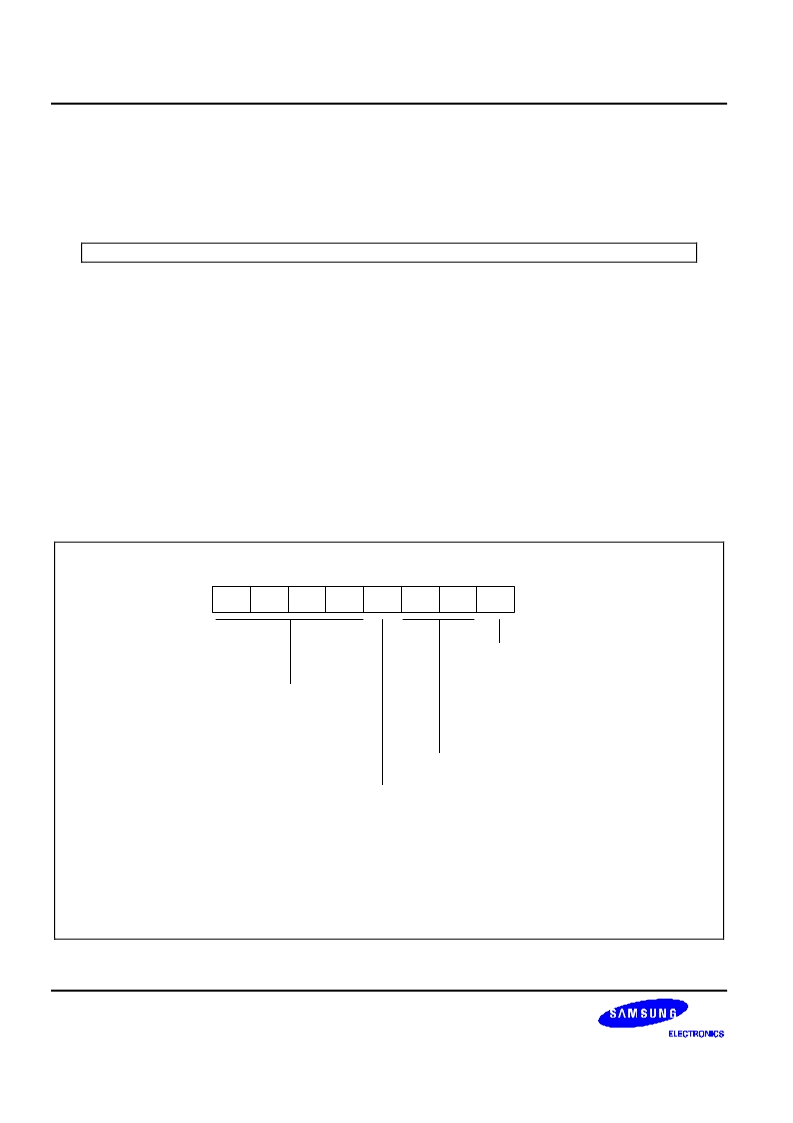
A/D Converter Control Register (ADCON)
D1H, Page0, R/W (EOC bit is read-only)
.7
.6
.5
.4
.3
.2
.1
.0
MSB
LSB
End-of-conversion bit:
0 = Not complete Conversion
1 = Complete Conversion
A/D input pin selection bits:
0000 = AD0
0001 = AD1
0010 = AD2
0011 = AD3
0100 = AD4
0101 = AD5
0110 = AD6
0111 = AD7
1000 = AD8
1001 = AD9
1010 = AD10
1011 = AD11
1100 = AD12
1101 = AD13
1110 = AD14
1111 = AD15
Clock Selection bits:
00 = fxx/16
01 = fxx/8
10 = fxx/4
11 = fxx/1
Figure 15-1. A/D Converter Control Register (ADCON)
相關(guān)PDF資料 |
PDF描述 |
|---|---|
| S3F49FAX | S3F49FAX for Compact Flash SPECIFICATION Revision 1.0 |
| S3F49FAXZA | S3F49FAX for Compact Flash SPECIFICATION Revision 1.0 |
| S3F49FAXZZ | S3F49FAX for Compact Flash SPECIFICATION Revision 1.0 |
| S413D | Fast Soft Recovery Rectifier |
| S414 | Fast Soft Recovery Rectifier |
相關(guān)代理商/技術(shù)參數(shù) |
參數(shù)描述 |
|---|---|
| S3F94A5XZZ-AO95 | 制造商:Samsung Semiconductor 功能描述:S3F94A5XZZ-AO95 |
| S3F94A5XZZ-AQ95 | 制造商:Samsung Semiconductor 功能描述:S3F94A5XZZ-AQ95 |
| S3F94A5XZZ-QZ85 | 制造商:Samsung Semiconductor 功能描述:S3F94A5XZZ-QZ85 |
| S3F94C4EZZ-DK94 | 制造商:Samsung Semiconductor 功能描述:SAMSUNG 8-BIT MC |
| S3F94C4EZZ-SK94 | 制造商:Samsung Semiconductor 功能描述:S3F94C4EZZ-SK94 |
發(fā)布緊急采購(gòu),3分鐘左右您將得到回復(fù)。