- 您現(xiàn)在的位置:買賣IC網(wǎng) > PDF目錄385768 > RF2469 (RF MICRO DEVICES INC) W-CDMA AND PCS LOW NOISE AMPLIFIER/MIXER DOWNCONVERTER PDF資料下載
參數(shù)資料
| 型號: | RF2469 |
| 廠商: | RF MICRO DEVICES INC |
| 元件分類: | 無繩電話/電話 |
| 英文描述: | W-CDMA AND PCS LOW NOISE AMPLIFIER/MIXER DOWNCONVERTER |
| 中文描述: | TELECOM, CELLULAR, RF AND BASEBAND CIRCUIT, QCC20 |
| 封裝: | 4 X 4 MM, LCC-20 |
| 文件頁數(shù): | 4/18頁 |
| 文件大小: | 255K |
| 代理商: | RF2469 |
Preliminary
8-36
RF2469
Rev A5 010717
8
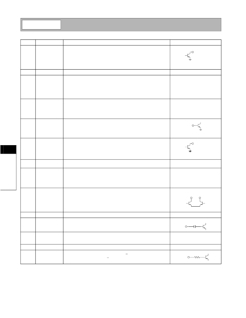
F
Pin
1
Function
LNA1 OUT
Description
LNA output pin. This is an open-collector output. Externally matched to
50
.
Interface Schematic
2
3
GND
VCC1
This pin is connected to the ground plane.
Supply voltage for LNA1. An external resistor is placed in series with
this pin to adjust the current and IIP3 of LNA1. A nominal value of
1.1k
sets the LNA1 current to 4.5mA with a minimum IIP3 of +7dBm.
External RF bypassing is required. The trace length between the
bypass caps and the pin should be minimized. Connect ground sides of
caps directly to ground.
Supply voltage for LNA2. An external resistor is placed in series with
this pin to adjust the current and IIP3 of LNA2. A nominal value of
2.4k
sets the LNA2 current to 1.6mA. External RF bypassing is
required. The trace length between the bypass caps and the pin should
be minimized. Connect ground sides of caps directly to ground.
RF input to LNA2. This pin is internally DC-biased and, if it is con-
nected to a device with DC present, should be DC-blocked with a
capacitor suitable for the frequency of operation.
4
VCC1
5
LNA2 IN
6
LNA2 OUT
LNA output pin. This is an open-collector output. In normal operation,
this pin is externally cascaded with pin 8 (MIX IN).
7
GND
Ground connection. For best performance, keep traces physically short
and connect directly to ground plane.
Mixer RF input pin. This pin requires a DC path to ground. In normal
operation, this pin is externally cascaded with pin 6 (LNA2 OUT). The
external match ensures a conjugate match between pin 6 and pin 8
while providing a DC path to ground for pin 8 and a DC-block between
pin 8 and pin 6.
IF output pin. The output is balanced. A current combiner external net-
work performs a differential to single-ended conversion and sets the
output impedance. There must be a DC path from V
CC
to this pin. This
is normally achieved with the current combiner network. A DC blocking
cap must be present if the IF filter input has a DC path to ground.
8
MIX IN
9
IF+
10
11
IF-
Same as pin 9, except complementary output.
See pin 9.
LO IN
Mixer LO single-ended input. The pin is internally DC-blocked. External
matching sets impedance.
12
VCC1
Supply voltage for LO buffer. External RF bypassing is required. The
trace length between the bypass caps and the pin should be minimized.
Connect ground sides of caps directly to ground.
This pin is connected to the ground plane.
13
14
GND
LNA2 BYP
Logic control for LNA2 gain. A logic high (>2.4V) places LNA2 in the
high gain mode. A logic low (<0.3V) place LNA2 in the bypass mode.
LNA1 OUT
LNA2 IN
LNA2 OUT
IF+
IF-
LO IN
LNA2 BYP
32 k
相關(guān)PDF資料 |
PDF描述 |
|---|---|
| RF2472 | 2.4GHZ LOW NOISE AMPLIFIER WITH ENABLE |
| RF2475 | DUAL-BAND LOW NOISE AMPLIFIER/MIXER WITH FREQUENCY DOUBLER |
| RF2480 | DIRECT QUADRATURE MODULATOR |
| RF2483 | LOW NOISE DUAL-BAND QUADRATURE MODULATOR WITH AGC |
| RF2484 | DIRECT QUADRATURE MODULATOR |
相關(guān)代理商/技術(shù)參數(shù) |
參數(shù)描述 |
|---|---|
| RF2471-000 | 功能描述:可復(fù)位保險絲 RoHS:否 制造商:Bourns 電流額定值: 電阻:7.5 Ohms 最大直流電壓: 保持電流:0.1 A 安裝風(fēng)格:SMD/SMT 端接類型:SMD/SMT 跳閘電流:0.6 A 引線間隔: 系列:MF-PSHT 工作溫度范圍:- 40 C to + 125 C |
| RF2472 | 制造商:RFMD 制造商全稱:RF Micro Devices 功能描述:2.4GHZ LOW NOISE AMPLIFIER WITH ENABLE |
| RF2472_06 | 制造商:RFMD 制造商全稱:RF Micro Devices 功能描述:2.4GHz LOW NOISE AMPLIFIER WITH ENABLE |
| RF2472_1 | 制造商:RFMD 制造商全稱:RF Micro Devices 功能描述:2.4GHz LOW NOISE AMPLIFIER WITH ENABLE |
| RF2472G | 制造商:RFMD 制造商全稱:RF Micro Devices 功能描述:2.4GHz LOW NOISE AMPLIFIER WITH ENABLE |
發(fā)布緊急采購,3分鐘左右您將得到回復(fù)。