- 您現(xiàn)在的位置:買(mǎi)賣(mài)IC網(wǎng) > PDF目錄368224 > PSD4235G2V -200V 100kRad Hi-Rel Single P-Channel TID Hardened MOSFET in a TO-254AA package; A JANSR2N7426 with Standard Packaging PDF資料下載
參數(shù)資料
| 型號(hào): | PSD4235G2V |
| 英文描述: | -200V 100kRad Hi-Rel Single P-Channel TID Hardened MOSFET in a TO-254AA package; A JANSR2N7426 with Standard Packaging |
| 中文描述: | Flash在系統(tǒng)編程(ISP)外設(shè)的16位微控制器(3.3V電源) |
| 文件頁(yè)數(shù): | 63/89頁(yè) |
| 文件大小: | 703K |
| 代理商: | PSD4235G2V |
第1頁(yè)第2頁(yè)第3頁(yè)第4頁(yè)第5頁(yè)第6頁(yè)第7頁(yè)第8頁(yè)第9頁(yè)第10頁(yè)第11頁(yè)第12頁(yè)第13頁(yè)第14頁(yè)第15頁(yè)第16頁(yè)第17頁(yè)第18頁(yè)第19頁(yè)第20頁(yè)第21頁(yè)第22頁(yè)第23頁(yè)第24頁(yè)第25頁(yè)第26頁(yè)第27頁(yè)第28頁(yè)第29頁(yè)第30頁(yè)第31頁(yè)第32頁(yè)第33頁(yè)第34頁(yè)第35頁(yè)第36頁(yè)第37頁(yè)第38頁(yè)第39頁(yè)第40頁(yè)第41頁(yè)第42頁(yè)第43頁(yè)第44頁(yè)第45頁(yè)第46頁(yè)第47頁(yè)第48頁(yè)第49頁(yè)第50頁(yè)第51頁(yè)第52頁(yè)第53頁(yè)第54頁(yè)第55頁(yè)第56頁(yè)第57頁(yè)第58頁(yè)第59頁(yè)第60頁(yè)第61頁(yè)第62頁(yè)當(dāng)前第63頁(yè)第64頁(yè)第65頁(yè)第66頁(yè)第67頁(yè)第68頁(yè)第69頁(yè)第70頁(yè)第71頁(yè)第72頁(yè)第73頁(yè)第74頁(yè)第75頁(yè)第76頁(yè)第77頁(yè)第78頁(yè)第79頁(yè)第80頁(yè)第81頁(yè)第82頁(yè)第83頁(yè)第84頁(yè)第85頁(yè)第86頁(yè)第87頁(yè)第88頁(yè)第89頁(yè)
63/89
PSD4235G2
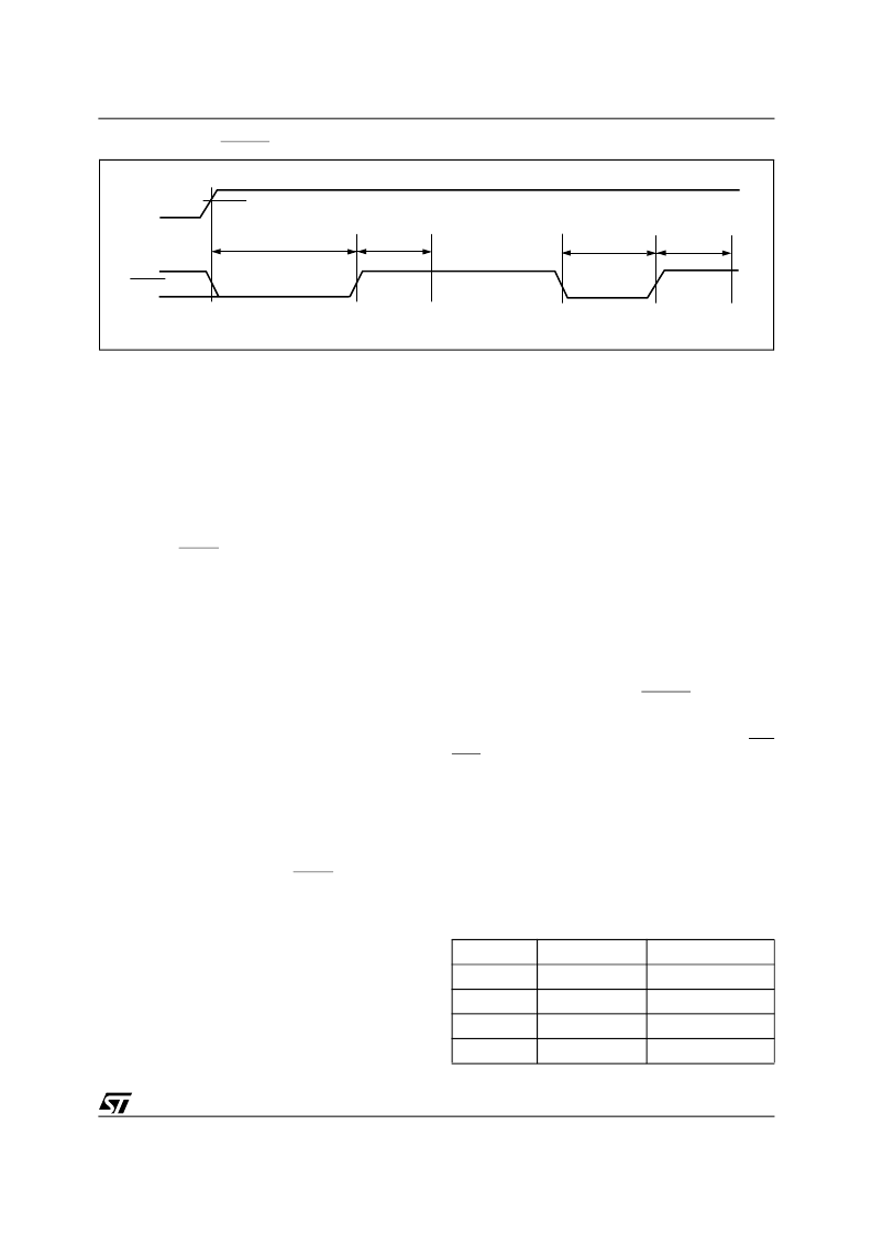
Figure 34. Reset (RESET) Timing
Programming In-Circuit using the JTAG Serial
Interface
The JTAG Serial Interface on the PSD can be en-
abled on Port E (see Table 52). All memory blocks
(primary Flash memory and secondary Flash
memory), PLD logic, and PSD Configuration bits
may be programmed through the JTAG-ISC Serial
Interface. A blank device can be mounted on a
printed circuit board and programmed using JTAG
In-System Programming (ISP).
The standard JTAG signals (IEEE 1149.1) are
TMS, TCK, TDI, and TDO. Two additional signals,
TSTAT and TERR, are optional JTAG extensions
used to speed up Program and Erase cycles.
By default, on a blank PSD (as shipped from the
factory, or after erasure), four pins on Port E are
enabled for the basic JTAG signals TMS, TCK,
TDI, and TDO.
See Application Note AN1153 for more details on
JTAG In-System Programming (ISP).
Standard JTAG Signals.
The standard JTAG
signals (TMS, TCK, TDI, and TDO) can be en-
abled by any of three different conditions that are
logically ORed. When enabled, TDI, TDO, TCK,
and TMS are inputs, waiting for a serial command
from an external JTAG controller device (such as
FlashLINK or Automated Test Equipment). When
the enabling command is received from the exter-
nal JTAG controller device, TDO becomes an out-
put and the JTAG channel is fully functional inside
the PSD. The same command that enables the
JTAG channel may optionally enable the two addi-
tional JTAG pins, TSTAT and TERR.
The following symbolic logic equation specifies the
conditions enabling the four basic JTAG pins
(TMS, TCK, TDI, and TDO) on their respective
Port E pins. For purposes of discussion, the logic
label JTAG_ON is used. When JTAG_ON is true,
the four pins are enabled for JTAG. When
JTAG_ON is false, the four pins can be used for
general PSD I/O.
JTAG_ON = PSDsoft Express_enabled +
/* An NVM configuration bit inside the
PSD is set by the designer in the
PSDsoft Express Configuration utility.
This dedicates the pins for JTAG at all
times (compliant with IEEE 1149.1 */
Microcontroller_enabled +
/* The microcontroller can set a bit at
run-time
by
writing
register, JTAG Enable. This register
is located at address CSIOP + offset
C7h. Setting the JTAG_ENABLE bit in
this register will enable the pins for
JTAG use. This bit is cleared by a PSD
reset or the microcontroller. See
Table 21 for bit definition. */
PSD_product_term_enabled;
/* A dedicated product term (PT) inside
the PSD can be used to enable the JTAG
pins. This PT has the reserved name
JTAGSEL. Once defined as a node in
PSDabel, the designer can write an
equation for JTAGSEL. This method is
used when the Port E JTAG pins are
multiplexed with other I/O signals. It
is recommended to tie logically the
node JTAGSEL to the JEN\ signal on the
Flashlink cable when multiplexing JTAG
signals. See Application Note 1153 for
details. */
The state of the PSD Reset (RESET) signal does
not interrupt (or prevent) JTAG operations if the
JTAG pins are dedicated by an NVM configuration
bit (via PSDsoft Express). However, Reset (RE-
SET) will prevent or interrupt JTAG operations if
the JTAG Enable Register (as shown in Table 21)
is used to enable the JTAG pins.
The PSD supports JTAG In-System-Programma-
bility (ISP) commands, but not Boundary Scan.
ST’s PSDsoft Express software tool and
FlashLINK JTAG programming cable implement
the JTAG In-System-Programmability (ISP) com-
mands.
to
the
PSD
Table 52. JTAG Port Signals
tNLNH-PO
Power-On Reset
tOPR
AI02866b
RESET
tNLNH
tNLNH-A
Warm Reset
tOPR
V
CC
V
CC
(min)
Port E Pin
JTAG Signals
Description
PE0
TMS
Mode Select
PE1
TCK
Clock
PE2
TDI
Serial Data In
PE3
TDO
Serial Data Out
相關(guān)PDF資料 |
PDF描述 |
|---|---|
| PSD4235G1-B-12J | Flash In-System Programmable ISP Peripherals For 16-bit MCUs 5V Supply |
| PSD4235F2-A-12J | Flash In-System Programmable ISP Peripherals For 16-bit MCUs 5V Supply |
| PSD4235G2-A-12J | Flash In-System Programmable ISP Peripherals For 16-bit MCUs 5V Supply |
| PSD4235G1-12B81 | Flash In-System-Programmable Peripherals for 16-Bit MCUs |
| PSD4235G1-12B81I | Flash In-System-Programmable Peripherals for 16-Bit MCUs |
相關(guān)代理商/技術(shù)參數(shù) |
參數(shù)描述 |
|---|---|
| PSD4235G2V-12UI | 功能描述:CPLD - 復(fù)雜可編程邏輯器件 3.3V 4M 120ns RoHS:否 制造商:Lattice 系列: 存儲(chǔ)類(lèi)型:EEPROM 大電池?cái)?shù)量:128 最大工作頻率:333 MHz 延遲時(shí)間:2.7 ns 可編程輸入/輸出端數(shù)量:64 工作電源電壓:3.3 V 最大工作溫度:+ 90 C 最小工作溫度:0 C 封裝 / 箱體:TQFP-100 |
| PSD4235G2V-90U | 功能描述:CPLD - 復(fù)雜可編程邏輯器件 3.3V 4M 90ns RoHS:否 制造商:Lattice 系列: 存儲(chǔ)類(lèi)型:EEPROM 大電池?cái)?shù)量:128 最大工作頻率:333 MHz 延遲時(shí)間:2.7 ns 可編程輸入/輸出端數(shù)量:64 工作電源電壓:3.3 V 最大工作溫度:+ 90 C 最小工作溫度:0 C 封裝 / 箱體:TQFP-100 |
| PSD4256G6V-10UI | 功能描述:CPLD - 復(fù)雜可編程邏輯器件 3.3V 8M 100ns RoHS:否 制造商:Lattice 系列: 存儲(chǔ)類(lèi)型:EEPROM 大電池?cái)?shù)量:128 最大工作頻率:333 MHz 延遲時(shí)間:2.7 ns 可編程輸入/輸出端數(shù)量:64 工作電源電壓:3.3 V 最大工作溫度:+ 90 C 最小工作溫度:0 C 封裝 / 箱體:TQFP-100 |
| PSD4-36 | 制造商:Tamura Corporation of America 功能描述: |
| PSD-45 | 制造商:MEANWELL 制造商全稱(chēng):Mean Well Enterprises Co., Ltd. 功能描述:45W DC-DC Single Output Switching Power Supply |
發(fā)布緊急采購(gòu),3分鐘左右您將得到回復(fù)。