- 您現(xiàn)在的位置:買賣IC網(wǎng) > PDF目錄368224 > PSD4235G2V -200V 100kRad Hi-Rel Single P-Channel TID Hardened MOSFET in a TO-254AA package; A JANSR2N7426 with Standard Packaging PDF資料下載
參數(shù)資料
| 型號(hào): | PSD4235G2V |
| 英文描述: | -200V 100kRad Hi-Rel Single P-Channel TID Hardened MOSFET in a TO-254AA package; A JANSR2N7426 with Standard Packaging |
| 中文描述: | Flash在系統(tǒng)編程(ISP)外設(shè)的16位微控制器(3.3V電源) |
| 文件頁(yè)數(shù): | 62/89頁(yè) |
| 文件大小: | 703K |
| 代理商: | PSD4235G2V |
第1頁(yè)第2頁(yè)第3頁(yè)第4頁(yè)第5頁(yè)第6頁(yè)第7頁(yè)第8頁(yè)第9頁(yè)第10頁(yè)第11頁(yè)第12頁(yè)第13頁(yè)第14頁(yè)第15頁(yè)第16頁(yè)第17頁(yè)第18頁(yè)第19頁(yè)第20頁(yè)第21頁(yè)第22頁(yè)第23頁(yè)第24頁(yè)第25頁(yè)第26頁(yè)第27頁(yè)第28頁(yè)第29頁(yè)第30頁(yè)第31頁(yè)第32頁(yè)第33頁(yè)第34頁(yè)第35頁(yè)第36頁(yè)第37頁(yè)第38頁(yè)第39頁(yè)第40頁(yè)第41頁(yè)第42頁(yè)第43頁(yè)第44頁(yè)第45頁(yè)第46頁(yè)第47頁(yè)第48頁(yè)第49頁(yè)第50頁(yè)第51頁(yè)第52頁(yè)第53頁(yè)第54頁(yè)第55頁(yè)第56頁(yè)第57頁(yè)第58頁(yè)第59頁(yè)第60頁(yè)第61頁(yè)當(dāng)前第62頁(yè)第63頁(yè)第64頁(yè)第65頁(yè)第66頁(yè)第67頁(yè)第68頁(yè)第69頁(yè)第70頁(yè)第71頁(yè)第72頁(yè)第73頁(yè)第74頁(yè)第75頁(yè)第76頁(yè)第77頁(yè)第78頁(yè)第79頁(yè)第80頁(yè)第81頁(yè)第82頁(yè)第83頁(yè)第84頁(yè)第85頁(yè)第86頁(yè)第87頁(yè)第88頁(yè)第89頁(yè)
PSD4235G2
62/89
Input Control Signals.
The PSD provides the
option to turn off the address input (A7-A0) and in-
put control signals (CNTL0, CNTL1, CNTL2, Ad-
dress Strobe (ALE/AS, PD0) and Write Enable
High-byte (WRH/DBE, PD3)) to the PLD to save
AC power consumption. These signals are inputs
to the PLD AND Array. During Power-down mode,
or, if any of them are not being used as part of the
PLD logic equation, these control signals should
be disabled to save AC power. They are discon-
nected from the PLD AND Array by setting bits 0,
2, 3, 4, 5 and 6 to a 1 in PMMR2.
Power On Reset, Warm Reset and Power-down
Power On Reset.
Upon Power-up, the PSD re-
quires a Reset (RESET) pulse of duration t
NLNH-
PO
(minimum 1 ms) after V
CC
is steady. During
this period, the device loads internal configura-
tions, clears some of the registers and sets the
Flash memory into Operating mode. After the ris-
ing edge of Reset (RESET), the PSD remains in
the Reset mode for an additional period, t
OPR
(maximum 120 ns), before the first memory ac-
cess is allowed.
The PSD Flash memory is reset to the Read mode
upon Power-up. Sector Select (FS0-FS7 and
CSBOOT0-CSBOOT3) must all be Low, Write
Strobe (WR/WRL, CNTL0) High, during Power On
Reset for maximum security of the data contents
and to remove the possibility of data being written
on the first edge of Write Strobe (WR/WRL,
CNTL0). Any Flash memory Write cycle initiation
is prevented automatically when V
CC
is below V
L-
KO
.
Warm Reset.
Once the device is up and running,
the device can be reset with a pulse of a much
shorter duration, t
NLNH
(minimum 150 ns). The
same t
OPR
period is needed before the device is
operational after warm reset. Figure 34 shows the
timing of the Power-up and warm reset.
I/O Pin, Register and PLD Status at Reset.
Ta-
ble 51 shows the I/O pin, register and PLD status
during Power On Reset, warm reset and Power-
down mode. PLD outputs are always valid during
warm reset, and they are valid in Power On Reset
once the internal PSD Configuration bits are load-
ed. This loading of PSD is completed typically long
before the V
CC
ramps up to operating level. Once
the PLD is active, the state of the outputs are de-
termined by equations specified in PSDsoft Ex-
press.
Reset of Flash Memory Erase and Program Cy-
cles.
An external Reset (RESET) also resets the
internal Flash memory state machine. During a
Flash memory Program or Erase cycle, Reset
(RESET) terminates the cycle and returns the
Flash memory to the Read mode within a period of
t
NLNH-A
(minimum 25
μ
s).
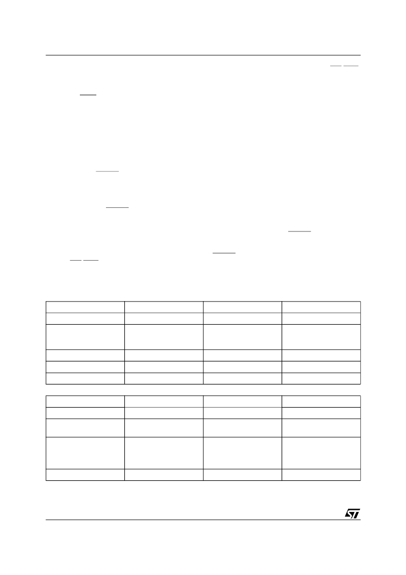
Table 51. Status During Power-On Reset, Warm Reset and Power-down Mode
Note: 1. The SR_code and Peripheral Mode bits in the VM Register are always cleared to 0 on Power-On Reset or Warm Reset.
Port Configuration
Power-On Reset
Warm Reset
Power-down Mode
MCU I/O
Input mode
Input mode
Unchanged
PLD Output
Valid after internal PSD
configuration bits are
loaded
Valid
Depends on inputs to PLD
(addresses are blocked in
PD mode)
Address Out
Tri-stated
Tri-stated
Not defined
Data Port
Tri-stated
Tri-stated
Tri-stated
Peripheral I/O
Tri-stated
Tri-stated
Tri-stated
Register
Power-On Reset
Warm Reset
Power-down Mode
PMMR0 and PMMR2
Cleared to 0
Unchanged
Unchanged
Macrocells Flip-flop status
Cleared to 0 by internal
Power-On Reset
Depends on .re and .pr
equations
Depends on .re and .pr
equations
VM Register
1
Initialized, based on the
selection in PSDsoft
Express
Configuration menu
Initialized, based on the
selection in PSDsoft
Express
Configuration menu
Unchanged
All other registers
Cleared to 0
Cleared to 0
Unchanged
相關(guān)PDF資料 |
PDF描述 |
|---|---|
| PSD4235G1-B-12J | Flash In-System Programmable ISP Peripherals For 16-bit MCUs 5V Supply |
| PSD4235F2-A-12J | Flash In-System Programmable ISP Peripherals For 16-bit MCUs 5V Supply |
| PSD4235G2-A-12J | Flash In-System Programmable ISP Peripherals For 16-bit MCUs 5V Supply |
| PSD4235G1-12B81 | Flash In-System-Programmable Peripherals for 16-Bit MCUs |
| PSD4235G1-12B81I | Flash In-System-Programmable Peripherals for 16-Bit MCUs |
相關(guān)代理商/技術(shù)參數(shù) |
參數(shù)描述 |
|---|---|
| PSD4235G2V-12UI | 功能描述:CPLD - 復(fù)雜可編程邏輯器件 3.3V 4M 120ns RoHS:否 制造商:Lattice 系列: 存儲(chǔ)類型:EEPROM 大電池?cái)?shù)量:128 最大工作頻率:333 MHz 延遲時(shí)間:2.7 ns 可編程輸入/輸出端數(shù)量:64 工作電源電壓:3.3 V 最大工作溫度:+ 90 C 最小工作溫度:0 C 封裝 / 箱體:TQFP-100 |
| PSD4235G2V-90U | 功能描述:CPLD - 復(fù)雜可編程邏輯器件 3.3V 4M 90ns RoHS:否 制造商:Lattice 系列: 存儲(chǔ)類型:EEPROM 大電池?cái)?shù)量:128 最大工作頻率:333 MHz 延遲時(shí)間:2.7 ns 可編程輸入/輸出端數(shù)量:64 工作電源電壓:3.3 V 最大工作溫度:+ 90 C 最小工作溫度:0 C 封裝 / 箱體:TQFP-100 |
| PSD4256G6V-10UI | 功能描述:CPLD - 復(fù)雜可編程邏輯器件 3.3V 8M 100ns RoHS:否 制造商:Lattice 系列: 存儲(chǔ)類型:EEPROM 大電池?cái)?shù)量:128 最大工作頻率:333 MHz 延遲時(shí)間:2.7 ns 可編程輸入/輸出端數(shù)量:64 工作電源電壓:3.3 V 最大工作溫度:+ 90 C 最小工作溫度:0 C 封裝 / 箱體:TQFP-100 |
| PSD4-36 | 制造商:Tamura Corporation of America 功能描述: |
| PSD-45 | 制造商:MEANWELL 制造商全稱:Mean Well Enterprises Co., Ltd. 功能描述:45W DC-DC Single Output Switching Power Supply |
發(fā)布緊急采購(gòu),3分鐘左右您將得到回復(fù)。