- 您現(xiàn)在的位置:買(mǎi)賣(mài)IC網(wǎng) > PDF目錄367738 > P87C554 (NXP Semiconductors N.V.) 80C51 8-bit microcontroller(80C51 8位微控制器) PDF資料下載
參數(shù)資料
| 型號(hào): | P87C554 |
| 廠商: | NXP Semiconductors N.V. |
| 英文描述: | 80C51 8-bit microcontroller(80C51 8位微控制器) |
| 中文描述: | 80C51的8位微控制器(80C51的8位微控制器) |
| 文件頁(yè)數(shù): | 64/78頁(yè) |
| 文件大小: | 393K |
| 代理商: | P87C554 |
第1頁(yè)第2頁(yè)第3頁(yè)第4頁(yè)第5頁(yè)第6頁(yè)第7頁(yè)第8頁(yè)第9頁(yè)第10頁(yè)第11頁(yè)第12頁(yè)第13頁(yè)第14頁(yè)第15頁(yè)第16頁(yè)第17頁(yè)第18頁(yè)第19頁(yè)第20頁(yè)第21頁(yè)第22頁(yè)第23頁(yè)第24頁(yè)第25頁(yè)第26頁(yè)第27頁(yè)第28頁(yè)第29頁(yè)第30頁(yè)第31頁(yè)第32頁(yè)第33頁(yè)第34頁(yè)第35頁(yè)第36頁(yè)第37頁(yè)第38頁(yè)第39頁(yè)第40頁(yè)第41頁(yè)第42頁(yè)第43頁(yè)第44頁(yè)第45頁(yè)第46頁(yè)第47頁(yè)第48頁(yè)第49頁(yè)第50頁(yè)第51頁(yè)第52頁(yè)第53頁(yè)第54頁(yè)第55頁(yè)第56頁(yè)第57頁(yè)第58頁(yè)第59頁(yè)第60頁(yè)第61頁(yè)第62頁(yè)第63頁(yè)當(dāng)前第64頁(yè)第65頁(yè)第66頁(yè)第67頁(yè)第68頁(yè)第69頁(yè)第70頁(yè)第71頁(yè)第72頁(yè)第73頁(yè)第74頁(yè)第75頁(yè)第76頁(yè)第77頁(yè)第78頁(yè)
Philips Semiconductors
Preliminary specification
80C554/83C554/87C554
80C51 8-bit microcontroller
16K/512 OTP/ROM/ROMless, 8 channel 10 bit A/D, I
2
C, PWM,
capture/compare, high I/O
1999 Apr 07
64
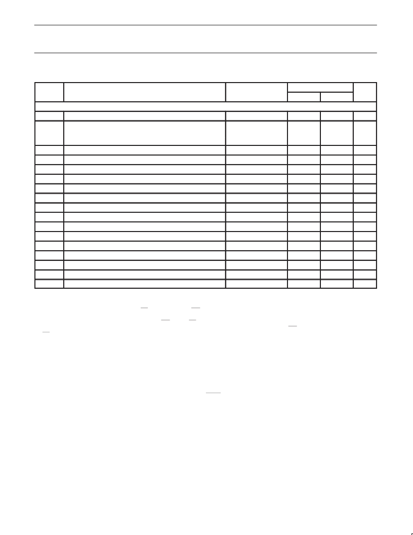
DC ELECTRICAL CHARACTERISTICS
(Continued)
TEST
LIMITS
SYMBOL
PARAMETER
CONDITIONS
MIN
MAX
UNIT
Analog Inputs (Continued)
AV
IN
AV
REF
Analog input voltage
AV
SS
–0.2
AV
DD
+0.2
V
Reference voltage:
AV
REF–
AV
REF+
Resistance between AV
REF+
and AV
REF–
Analog input capacitance
AV
SS
–0.2
V
V
AV
DD
+0.2
50
R
REF
C
IA
t
ADS
t
ADS8
t
ADC
t
ADC8
DL
e
IL
e
IL
e8
OS
e
OS
e8
G
e
A
e
M
CTC
C
t
NOTES FOR DC ELECTRICAL CHARACTERISTICS:
1. See Figures 57 through 61 for I
DD
test conditions.
2. The operating supply current is measured with all output pins disconnected; XTAL1 driven with t
r
= t
f
= 10ns; V
IL
= V
SS
+ 0.5V;
V
IH
= V
DD
– 0.5V; XTAL2 not connected; EA = RST = Port 0 = EW = V
DD
; STADC = V
SS
.
3. The idle mode supply current is measured with all output pins disconnected; XTAL1 driven with t
r
= t
f
= 10ns; V
IL
= V
SS
+ 0.5V;
V
IH
= V
DD
– 0.5V; XTAL2 not connected; Port 0 = EW = V
DD
; EA = RST = STADC = V
SS
.
4. The power-down current is measured with all output pins disconnected; XTAL2 not connected; Port 0 = EW = V
DD
;
EA = RST = STADC = XTAL1 = V
.
5. The input threshold voltage of P1.6 and P1.7 (SIO1) meets the I
2
C specification, so an input voltage below 1.5V will be recognized as a logic
0 while an input voltage above 3.0V will be recognized as a logic 1.
6. Pins of ports 1 (except P1.6, P1.7), 2, 3, and 4 source a transition current when they are being externally driven from 1 to 0. The transition
current reaches its maximum value when V
IN
is approximately 2V.
7. Capacitive loading on ports 0 and 2 may cause spurious noise to be superimposed on the V
OL
s of ALE and ports 1 and 3. The noise is due
to external bus capacitance discharging into the port 0 and port 2 pins when these pins make 1-to-0 transitions during bus operations. In the
worst cases (capacitive loading > 100pF), the noise pulse on the ALE pin may exceed 0.8V. In such cases, it may be desirable to qualify
ALE with a Schmitt Trigger, or use an address latch with a Schmitt Trigger STROBE input. I
OL
can exceed these conditions provided that no
single output sinks more than 5mA and no more than two outputs exceed the test conditions.
8. Capacitive loading on ports 0 and 2 may cause the V
OH
on ALE and PSEN to momentarily fall below the 0.9V
DD
specification when the
address bits are stabilizing.
9. The following condition must not be exceeded: V
DD
– 0.2V < AV
DD
< V
DD
+ 0.2V.
10.Conditions: AV
REF–
= 0V; AV
DD
= 5.0V. Measurement by continuous conversion of AV
IN
= –20mV to 5.12V in steps of 0.5mV, derivating
parameters from collected conversion results of ADC. AV
REF+
(87C554) = 4.977V. ADC is monotonic with no missing codes.
11. The differential non-linearity (DL
e
) is the difference between the actual step width and the ideal step width. (See Figure 48.)
12.The ADC is monotonic; there are no missing codes.
13.The integral non-linearity (IL
) is the peak difference between the center of the steps of the actual and the ideal transfer curve after
appropriate adjustment of gain and offset error. (See Figure 48.)
14.The offset error (OS
) is the absolute difference between the straight line which fits the actual transfer curve (after removing gain error), and
a straight line which fits the ideal transfer curve. (See Figure 48.)
15.The gain error (G
e
) is the relative difference in percent between the straight line fitting the actual transfer curve (after removing offset error),
and the straight line which fits the ideal transfer curve. Gain error is constant at every point on the transfer curve. (See Figure 48.)
16.The absolute voltage error (A
e
) is the maximum difference between the center of the steps of the actual transfer curve of the non-calibrated
ADC and the ideal transfer curve.
17.This should be considered when both analog and digital signals are simultaneously input to port 5.
18.This parameter is guaranteed by design and characterized, but is not production tested.
10
k
15
pF
Sampling time (10 bit mode)
8t
CY
5t
CY
50t
CY
24t
CY
±
1
±
2
±
1
±
2
±
1
±
0.4
±
3
±
1
μ
s
μ
s
μ
s
μ
s
Sampling time (8 bit mode)
Conversion time (including sampling time, 10 bit mode)
Conversion time (including sampling time, 8 bit mode)
Differential non-linearity
10, 11, 12
Integral non-linearity
10, 13
(10 bit mode)
LSB
LSB
Integral non-linearity (8 bit mode)
Offset error
10, 14
(10 bit mode)
LSB
LSB
Offset error (8 bit mode)
Gain error
10, 15
Absolute voltage error
10, 16
LSB
%
LSB
Channel to channel matching
Crosstalk
between inputs of port 5
17, 18
LSB
0–100kHz
–60
dB
相關(guān)PDF資料 |
PDF描述 |
|---|---|
| P87C654X2 | Octal Edge-Triggered D-Type Flip-Flops with 3-State Outputs 20-CDIP -55 to 125 |
| P83C654X2 | 80C51 8-bit microcontroller family 16 kB OTP/ROM, 256B RAM, low voltage (2.7 to 5.5 V), low power, high speed (30/33 MHz) |
| P83C654EFP | CONN HEADER 11POS SGL PCB 30GOLD |
| P83C654EFPN | CONN HEADER 13POS SGL PCB 30GOLD |
| P83C654EHA | CMOS single-chip 8-bit microcontroller |
相關(guān)代理商/技術(shù)參數(shù) |
參數(shù)描述 |
|---|---|
| P87C554SBAA | 制造商:NXP Semiconductors 功能描述:MCU 8-Bit 87C 80C51 CISC 16KB EPROM 5V 68-Pin PLCC |
| P87C554SBAA,512 | 功能描述:8位微控制器 -MCU 80C51 16K/512 OTP RoHS:否 制造商:Silicon Labs 核心:8051 處理器系列:C8051F39x 數(shù)據(jù)總線寬度:8 bit 最大時(shí)鐘頻率:50 MHz 程序存儲(chǔ)器大小:16 KB 數(shù)據(jù) RAM 大小:1 KB 片上 ADC:Yes 工作電源電壓:1.8 V to 3.6 V 工作溫度范圍:- 40 C to + 105 C 封裝 / 箱體:QFN-20 安裝風(fēng)格:SMD/SMT |
| P87C554SBBD | 制造商:PHILIPS 制造商全稱(chēng):NXP Semiconductors 功能描述:80C51 8-bit microcontroller . 6 clock operation 16K/512 OTP/ROM/ROMless, 7 channel 10 bit A/D, I2C, PWM, capture/compare, high I/O, 64L LQFP |
| P87C554SFAA | 制造商:PHILIPS 制造商全稱(chēng):NXP Semiconductors 功能描述:80C51 8-bit microcontroller ? 12 clock operation 16K/512 OTP/RAM 8 channel 10-bit A/D, I2C, PWM, capture/compare, high I/O |
| P87C554SFAA,512 | 功能描述:8位微控制器 -MCU 80C51 16K/512 OTP RoHS:否 制造商:Silicon Labs 核心:8051 處理器系列:C8051F39x 數(shù)據(jù)總線寬度:8 bit 最大時(shí)鐘頻率:50 MHz 程序存儲(chǔ)器大小:16 KB 數(shù)據(jù) RAM 大小:1 KB 片上 ADC:Yes 工作電源電壓:1.8 V to 3.6 V 工作溫度范圍:- 40 C to + 105 C 封裝 / 箱體:QFN-20 安裝風(fēng)格:SMD/SMT |
發(fā)布緊急采購(gòu),3分鐘左右您將得到回復(fù)。