- 您現(xiàn)在的位置:買賣IC網(wǎng) > PDF目錄361102 > NCP5218 (ON SEMICONDUCTOR) 2−in−1 Notebook DDR Power Controller PDF資料下載
參數(shù)資料
| 型號: | NCP5218 |
| 廠商: | ON SEMICONDUCTOR |
| 英文描述: | 2−in−1 Notebook DDR Power Controller |
| 文件頁數(shù): | 4/31頁 |
| 文件大小: | 463K |
| 代理商: | NCP5218 |
第1頁第2頁第3頁當(dāng)前第4頁第5頁第6頁第7頁第8頁第9頁第10頁第11頁第12頁第13頁第14頁第15頁第16頁第17頁第18頁第19頁第20頁第21頁第22頁第23頁第24頁第25頁第26頁第27頁第28頁第29頁第30頁第31頁
NCP5218
http://onsemi.com
4
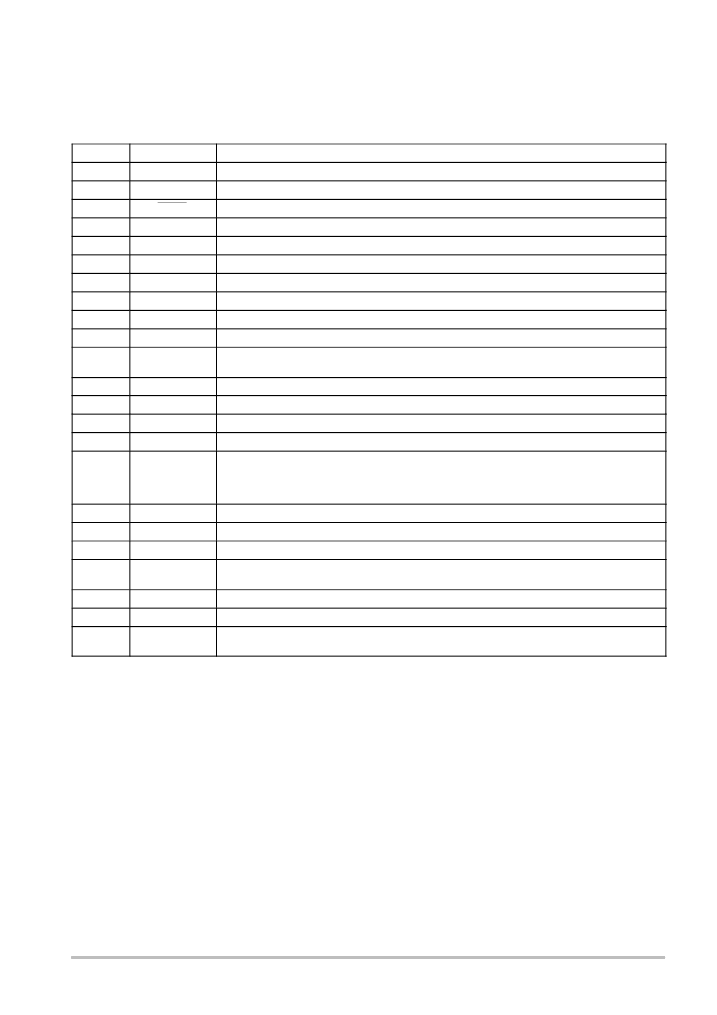
PIN FUNCTION DESCRIPTION
Pin
Symbol
Description
1
VDDQEN
V
DDQ
regulator enable input. High to enable.
2
VTTEN
V
TT
regulator enable input. High to enable.
3
FPWM
Forced PWM enable input. Low to enable forced PWM mode and disable power
saving mode.
4
SS
V
DDQ
Soft
start capacitor connection to ground.
5
VTTGND
Power ground for the V
TT
regulator.
6
VTT
V
TT
regulator output.
7
VTTI
Power input for V
TT
regulator which is normally connected to the V
DDQ
output of the buck regulator.
8
FBVTT
V
TT
regulator feedback pin for closed loop regulation.
9
AGND
Analog ground connection and remote ground sense.
10
DDQREF
External reference input which is used to regulate V
TT
and V
TTREF
to 1/2V
DDQREF
.
11
VCCA
5.0 V supply input for the IC’s control and logic section, which is monitored by undervoltage lock out
circuitry.
12
COMP
V
DDQ
error amplifier compensation node.
13
FBDDQ
V
DDQ
regulator feedback pin for closed loop regulation.
14
VTTREF
DDR reference voltage output.
15
PGOOD
Power good signal open
drain output.
16
OCDDQ
Overcurrent sense and program input for the high
side FET of V
DDQ
regulator.
Also the battery voltage
input for the internal ramp generator to implement the voltage feedforward rejection to the input voltage
variation. This pin must be connected to the V
IN
through a resistor to perform the current limit and
voltage feedforward functions.
17
BOOST
Positive supply input for high
side gate driver of V
DDQ
regulator and boost capacitor connection.
18
TGDDQ
Gate driver output for V
DDQ
regulator high
side N
Channel power FET.
19
SWDDQ
V
DDQ
regulator inductor driven node, return for high
side gate driver, and current limit sense input.
20
VCCP
Power supply for the V
DDQ
regulator low
side gate driver and also supply voltage for the bootstrap
capacitor of the V
DDQ
regulator high
side gate driver supply.
21
BGDDQ
Gate driver output for V
DDQ
regulator low
side N
Channel power FET.
22
PGND
Power ground for the V
DDQ
regulator.
23
THPAD
Copper pad on bottom of IC used for heatsinking. This pin should be connected to the ground plane
under the IC.
相關(guān)PDF資料 |
PDF描述 |
|---|---|
| NCP5218MNR2G | 2−in−1 Notebook DDR Power Controller |
| NCP5220 | 3−in−1 PWM Dual Buck and Linear Power Controller |
| NCP5220MNR2 | 3−in−1 PWM Dual Buck and Linear Power Controller |
| NCP5220MNR2G | 3−in−1 PWM Dual Buck and Linear Power Controller |
| NCP5306 | Three−Phase VRM 9.0 Buck Controller |
相關(guān)代理商/技術(shù)參數(shù) |
參數(shù)描述 |
|---|---|
| NCP5218MNR2G | 功能描述:電壓模式 PWM 控制器 2IN1 NOTEBK DDR CNTL RoHS:否 制造商:Texas Instruments 輸出端數(shù)量:1 拓?fù)浣Y(jié)構(gòu):Buck 輸出電壓:34 V 輸出電流: 開關(guān)頻率: 工作電源電壓:4.5 V to 5.5 V 電源電流:600 uA 最大工作溫度:+ 125 C 最小工作溫度:- 40 C 封裝 / 箱體:WSON-8 封裝:Reel |
| NCP5220 | 制造商:ONSEMI 制造商全稱:ON Semiconductor 功能描述:3−in−1 PWM Dual Buck and Linear Power Controller |
| NCP5220AMNR2 | 功能描述:DC/DC 開關(guān)控制器 3-in-1 PWM Dual Buck RoHS:否 制造商:Texas Instruments 輸入電壓:6 V to 100 V 開關(guān)頻率: 輸出電壓:1.215 V to 80 V 輸出電流:3.5 A 輸出端數(shù)量:1 最大工作溫度:+ 125 C 安裝風(fēng)格: 封裝 / 箱體:CPAK |
| NCP5220AMNR2G | 功能描述:DC/DC 開關(guān)控制器 ANA DDR PWER CNTRLR RoHS:否 制造商:Texas Instruments 輸入電壓:6 V to 100 V 開關(guān)頻率: 輸出電壓:1.215 V to 80 V 輸出電流:3.5 A 輸出端數(shù)量:1 最大工作溫度:+ 125 C 安裝風(fēng)格: 封裝 / 箱體:CPAK |
| NCP5220MNR2 | 功能描述:DC/DC 開關(guān)控制器 3-in-1 PWM Dual Buck RoHS:否 制造商:Texas Instruments 輸入電壓:6 V to 100 V 開關(guān)頻率: 輸出電壓:1.215 V to 80 V 輸出電流:3.5 A 輸出端數(shù)量:1 最大工作溫度:+ 125 C 安裝風(fēng)格: 封裝 / 箱體:CPAK |
發(fā)布緊急采購,3分鐘左右您將得到回復(fù)。