- 您現(xiàn)在的位置:買賣IC網(wǎng) > PDF目錄359233 > MT8930C (Zarlink Semiconductor Inc.) Subscriber Network Interface Circuit PDF資料下載
參數(shù)資料
| 型號: | MT8930C |
| 廠商: | Zarlink Semiconductor Inc. |
| 英文描述: | Subscriber Network Interface Circuit |
| 中文描述: | 用戶網(wǎng)絡接口電路 |
| 文件頁數(shù): | 2/41頁 |
| 文件大?。?/td> | 2516K |
| 代理商: | MT8930C |
第1頁當前第2頁第3頁第4頁第5頁第6頁第7頁第8頁第9頁第10頁第11頁第12頁第13頁第14頁第15頁第16頁第17頁第18頁第19頁第20頁第21頁第22頁第23頁第24頁第25頁第26頁第27頁第28頁第29頁第30頁第31頁第32頁第33頁第34頁第35頁第36頁第37頁第38頁第39頁第40頁第41頁

MT8930C
Data Sheet
2
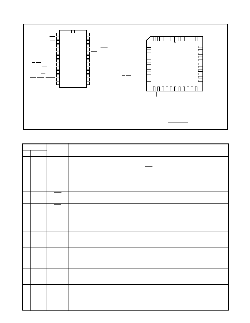
Figure 2 - Pin Connections
Pin Description
Pin #
Name
Description
DIP
1
PLCC
2
HALF
HALF Input/Output:
this is an input in NT mode and an output in TE mode identifying
which half of the S-interface frame is currently being written/read over the ST-BUS
(HALF = 0 sampled on the falling edge of C4b within the frame pulse low window,
identifies the information to be transmitted/received in the first half of the S-Bus frame
while HALF = 1 identifies the information to be transmitted/received into the second half
of the S-Bus frame). Tying this pin to V
SS
or V
DD
in NT mode will allow the device to
free run. This signal can also be accessed from the ST-BUS C-channel.
2
3
C4b
4.096 MHz Clock:
a 4.096 MHz ST-BUS Data Clock input in NT mode.
In TE mode, a 4.096 MHz output clock phase-locked to the line data signal.
3
4
F0b
Frame Pulse:
an active low frame pulse input indicating the beginning of active ST-
BUS channel times in NT mode. Frame pulse output in TE mode.
4
7
F0od
Delayed Frame Pulse Output:
an active low delayed frame pulse output indicating
the end of active ST-BUS channels for this device. Can be used to daisy chain
to other ST-BUS devices to share an ST-BUS stream.
Data ST-BUS Input:
a 2048 kbit/s serial PCM/data ST-BUS input with D, C, B1, and B2
channels assigned to the first four timeslots. These channels contain data to be
transmitted on the line and chip control information.
Data ST-BUS Output:
a 2048 kbit/s serial PCM/data ST-BUS output with D, C, B1 and
B2 channels assigned to the first four timeslots respectively. The remaining timeslots
are placed into high impedance. These channels contain data received from the line
and chip status information.
Controller Mode Select Input:
when high, microprocessor control is selected. When
low the controllerless mode is enabled and the microport pins are redefined as control
inputs and status outputs.
TE Clock/Network Termination Mode Select Input.
For TE mode, this pin must be
tied to V
SS
or to a 4.096 MHz clock (a clock is required for standard ISDN TE
applications). For NT mode, this pin must be tied to V
DD
. Refer to “ST-BUS Interface”
section for further explanation. A pull-up resistor is needed when driven by a TTL
device.
5
8
DSTi
6
9
DSTo
7
13
Cmode
8
14
CK/NT
1
2
3
4
5
6
7
8
9
10
11
12
13
14
15
16
17
18
19
20
28
27
26
25
24
23
22
21
HALF
C4b
F0b
F0od
DSTi
DSTo
Cmode
CK/NT
R/W/WR, AFT/PRI
DS/RD, DinB
AS/ALE, P/SC
CS, DReq
IRQ/NDA, DCack
VSS
VDD
VBias
LTx
LRx
STAR/Rsto
Rsti
AD7, DR
AD6, AR
AD5, M/S
AD4, MCH
AD3, MFR
AD2, SYNC/BA
AD1, IS1
AD0, IS0
28 PIN PDIP
44 PIN PLCC
N
N
C
F
H
V
V
L
N
L
NC
STAR/Rsto
Rsti
NC
AD7, DR
AD6, AR
NC
AD5, M/S
AD4, MCH
AD3, MFR
NC
F0od
DSTi
DSTo
NC
NC
NC
Cmode
CK/NT
NC
R/W/WR, AFT/PRI
DS/RD, DinB
N
A
C
I
V
A
A
A
N
N
N
N
1
6 5 4 3 2
7
8
9
10
11
12
13
14
15
16
17
4443424140
39
38
37
36
35
34
33
32
31
30
29
23
1819202122
2425262728
相關(guān)PDF資料 |
PDF描述 |
|---|---|
| MT8930CE | Subscriber Network Interface Circuit |
| MT8930CP | Subscriber Network Interface Circuit |
| MT8931C | Subscriber Network Interface Circuit |
| MT8931CE | Subscriber Network Interface Circuit |
| MT8931CP | Subscriber Network Interface Circuit |
相關(guān)代理商/技術(shù)參數(shù) |
參數(shù)描述 |
|---|---|
| MT8930C-1 | 制造商:MITEL 制造商全稱:Mitel Networks Corporation 功能描述:CMOS ST-BUS⑩ FAMILY Subscriber Network Interface Circuit |
| MT8930CC | 制造商:MITEL 制造商全稱:Mitel Networks Corporation 功能描述:CMOS ST-BUS⑩ FAMILY Subscriber Network Interface Circuit Preliminary Information |
| MT8930CE | 制造商:ZARLINK 制造商全稱:Zarlink Semiconductor Inc 功能描述:Subscriber Network Interface Circuit |
| MT8930CP | 制造商:ZARLINK 制造商全稱:Zarlink Semiconductor Inc 功能描述:Subscriber Network Interface Circuit |
| MT8930CPR | 制造商:Microsemi Corporation 功能描述: |
發(fā)布緊急采購,3分鐘左右您將得到回復。