- 您現(xiàn)在的位置:買賣IC網(wǎng) > PDF目錄299522 > MT49H8M36HU-33 8M X 36 DDR DRAM, 0.3 ns, PBGA144 PDF資料下載
參數(shù)資料
| 型號(hào): | MT49H8M36HU-33 |
| 元件分類: | DRAM |
| 英文描述: | 8M X 36 DDR DRAM, 0.3 ns, PBGA144 |
| 封裝: | FBGA-144 |
| 文件頁(yè)數(shù): | 72/76頁(yè) |
| 文件大小: | 2659K |
| 代理商: | MT49H8M36HU-33 |
第1頁(yè)第2頁(yè)第3頁(yè)第4頁(yè)第5頁(yè)第6頁(yè)第7頁(yè)第8頁(yè)第9頁(yè)第10頁(yè)第11頁(yè)第12頁(yè)第13頁(yè)第14頁(yè)第15頁(yè)第16頁(yè)第17頁(yè)第18頁(yè)第19頁(yè)第20頁(yè)第21頁(yè)第22頁(yè)第23頁(yè)第24頁(yè)第25頁(yè)第26頁(yè)第27頁(yè)第28頁(yè)第29頁(yè)第30頁(yè)第31頁(yè)第32頁(yè)第33頁(yè)第34頁(yè)第35頁(yè)第36頁(yè)第37頁(yè)第38頁(yè)第39頁(yè)第40頁(yè)第41頁(yè)第42頁(yè)第43頁(yè)第44頁(yè)第45頁(yè)第46頁(yè)第47頁(yè)第48頁(yè)第49頁(yè)第50頁(yè)第51頁(yè)第52頁(yè)第53頁(yè)第54頁(yè)第55頁(yè)第56頁(yè)第57頁(yè)第58頁(yè)第59頁(yè)第60頁(yè)第61頁(yè)第62頁(yè)第63頁(yè)第64頁(yè)第65頁(yè)第66頁(yè)第67頁(yè)第68頁(yè)第69頁(yè)第70頁(yè)第71頁(yè)當(dāng)前第72頁(yè)第73頁(yè)第74頁(yè)第75頁(yè)第76頁(yè)
PDF: 09005aef80a41b59/Source: 09005aef809f284b
Micron Technology, Inc., reserves the right to change products or specifications without notice.
288Mb_RLDRAM_II_CIO.Core.fm - Rev B 5/08 EN
73
2003 Micron Technology, Inc. All rights reserved.
288Mb: x9, x18, x36 2.5V VEXT, 1.8V VDD, HSTL, CIO, RLDRAM II
IEEE 1149.1 Serial Boundary Scan (JTAG)
Notes:
1. All voltages referenced to VSS (GND).
2. Overshoot = VIH(AC)
≤ VDD + 0.7V for t ≤ tCK/2; undershoot = VIL(AC) ≥ –0.5V for t ≤ tCK/2;
during normal operation, VDDQ must not exceed VDD.
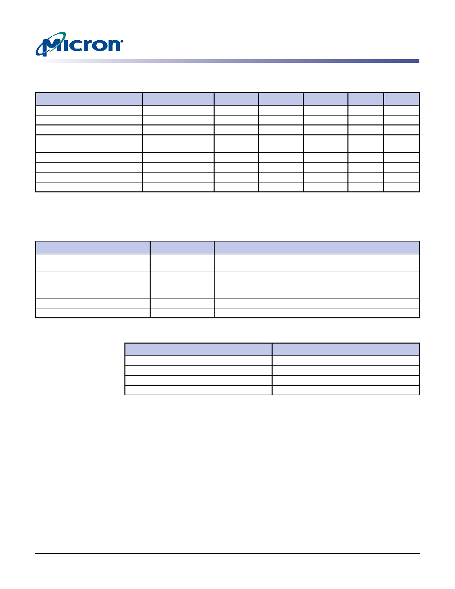
Table 25:
TAP DC Electrical Characteristics and Operating Conditions
+0°C
≤ T
C ≤ +95°C; +1.7V ≤ VDD ≤ +1.9V, unless otherwise noted
Description
Condition
Symbol
Min
Max
Units
Notes
Input high (logic 1) voltage
VIH
VREF + 0.15
VDD + 0.3
V
Input low (logic 0) voltage
VIL
VSSQ - 0.3
VREF - 0.15
V
Input leakage current
0V
≤ VIN ≤ VDD
ILI
–5.0
5.0
A
Output leakage current
Output disabled,
0V
≤ VIN ≤ VDDQ
ILO
–5.0
5.0
A
Output low voltage
IOLC = 100A
VOL10.2
V
Output low voltage
IOLT = 2mA
VOL20.4
V
Output high voltage
|IOHC| = 100A
VOH1VDDQ - 0.2
V
Output high voltage
|IOHT| = 2mA
VOH2VDDQ - 0.4
V
Table 26:
Identification Register Definitions
Instruction Field
All Devices
Description
Revision number (31:28)
abcd
ab = die revision
cd = 00 for x9, 01 for x18, 10 for x36
Device ID (27:12)
00jkidef10100111
def = 000 for 288Mb, 001 for 576Mb
i = 0 for common I/O, 1 for separate I/O
jk = 01 for RLDRAM II, 00 for RLDRAM
Micron JEDEC ID code (11:1)
00000101100
Allows unique identification of RLDRAM vendor
ID register presence indicator (0)
1
Indicates the presence of an ID register
Table 27:
Scan Register Sizes
Register Name
Bit Size
Instruction
8
Bypass
1
ID
32
Boundary scan
113
相關(guān)PDF資料 |
PDF描述 |
|---|---|
| MT4C1024DJ-6L | 1M X 1 FAST PAGE DRAM, 60 ns, PDSO20 |
| MT4C2M8A1DJ-7STR | 2M X 8 FAST PAGE DRAM, 70 ns, PDSO28 |
| MT4LC1M16C5TG-8S | 1M X 16 FAST PAGE DRAM, 80 ns, PDSO44 |
| MT4LC2M8A1DJ-6TR | 2M X 8 FAST PAGE DRAM, 60 ns, PDSO28 |
| MT52C9012DJ-25 | 1K X 9 OTHER FIFO, 25 ns, PDSO28 |
相關(guān)代理商/技術(shù)參數(shù) |
參數(shù)描述 |
|---|---|
| MT49H8M36HU-33 IT | 制造商:Micron Technology Inc 功能描述: |
| MT49H8M36HU-5 | 制造商:Micron Technology Inc 功能描述: |
| MT4A5 | 制造商:EDAL 制造商全稱:EDAL 功能描述:SILICON FAST RECOVERY 3.0 AMP DIODES |
發(fā)布緊急采購(gòu),3分鐘左右您將得到回復(fù)。